The ABCs of LEDs – Yield & Exclusion Zone
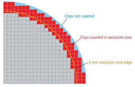
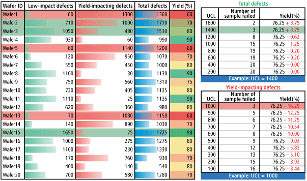
Y – Yield In order for LED manufacturers to stay competitive in this dynamic environment, they need to have a comprehensive in-line process ...
Posted by Janine Powell on
Y – Yield In order for LED manufacturers to stay competitive in this dynamic environment, they need to have a comprehensive in-line process ...
Posted by Janine Powell on
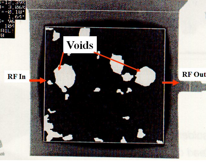
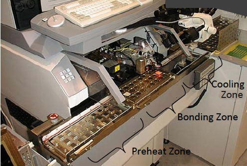
Eutectic bonding of Au-backed MMIC (Monolithic Microwave Integrated Circuits) power amplifiers presents a unique challenge due to the thin, ...
Posted by Janine Powell on
W – Wafer While the microelectronics industry is working hard to develop low-cost LED packaging methods—such as with thermally and ...
Posted by Janine Powell on
[For the English version, click here.] Традиционно, ультразвуковая микросварка предполагает разварку перемычек с кристалла на подложку. ...
Posted by Janine Powell on
U – Uniformity We are seeing more and more innovation in form factor and functionality in solid-state lighting products as lighting ...
Posted by Janine Powell on
Returning to our series on everything LEDs, we will pick back up at letters “S” and “T” with substrates and thermal/temperature sensitive. ...
Posted by Janine Powell on

Introduction to the Series With so much important technological history tied to Hughes Aircraft, it’s hard to believe that more has not ...
Posted by Janine Powell on
When discussing the hot topic of LEDs, quality and reliability become two major factors. Without either of these qualities, LEDs would have ...
Posted by Janine Powell on
Although there is continued effort in the semiconductor packaging industry to reduce package size along with the never-ending pursuit of ...
Posted by Janine Powell on
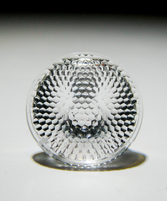
O – Optics The purpose of an optical component is to manipulate light. Typically, when we think of LED optics, what comes to mind is a ...
Posted by Janine Powell on
By submitting this form, I agree to receive information about Palomar Technologies's products by email. I understand I can opt-out any time.