
Working with Palomar Technologies, photonics device manufacturers can:
- Optimize return on investment with automated packaging solutions.
- Manufacture high-reliability photonics packaging providing for greater longevity.
- Reduced cost of ownership with flexible packaging assembly solutions, which can operate in R&D up to production environments.
With the push toward smart cities, autonomous vehicles, and 5G, the demand for connected devices and higher capacity networks is steadily growing, thereby increasing the need for light-enabled products and services, ushering photonics into a position of prominence in the world economy. Miniaturization and reduced foot print, reduced power consumption, reduced BOM & assembly costs are among the market challenges.
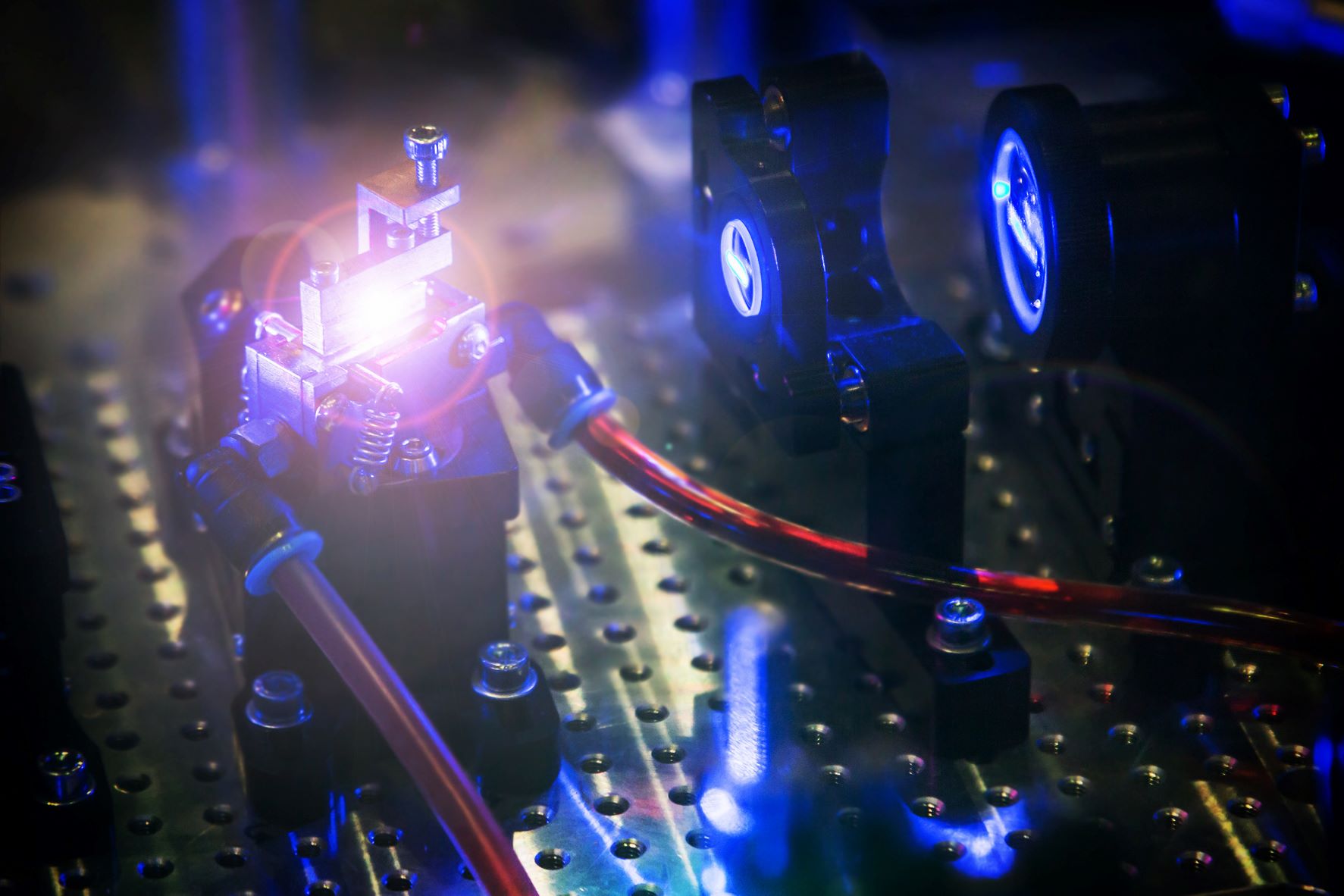
While 80% of the photonics market is optical and data transceivers, light-emitting diodes, quantum technologies, laser diode assemblies, high power laser modules, MEMS devices, bio-photonics, 5G, and all types of sensors make up a growing part. This growth puts strains on the manufacturing of these devices.
Packaging Assembly Challenges:
- Complicated assembly process (a typical 100G transceiver uses about 30 processes to build)
- Extreme number of components to bond (~70 components)
- Up to 5 different die bonding techniques
Palomar provides a range of flexible packaging solutions for photonics applications. The Palomar 3880-II Die Bonder offers the perfect balance of accuracy, throughput and flexibility. Using the 3880, 5μm TEC and CoC tack bonding, packages are fed into the SST 8300 Automated Vacuum Pressure Soldering System for void free, high-reliability, high-thermal stability applications. The Palomar 8100 Wire/Ball Bonder feeds the 3880 with accurate planar Au ball bumps in preparation for successful PiC flip chip thermos compressions applications.
Contact Us to Discuss Your Application