Y – Yield
In order for LED manufacturers to stay competitive in this dynamic environment, they need to have a comprehensive in-line process control strategy to improve the yield and drive down the cost of LEDs and SSL end products.
Yield refers to the measure of chips that function correctly. Generally yield is simply the number of good die divided by the total number of die. Defects with higher kill ratio have more negative impact on the yield. One does not find wafers that have high yield-impacting defect counts with high yields. As yield impacting defect counts increase, the yield decreases. A method of separating yield-impacting defects from nuisance defects is needed.
|
Controlling the eutectic attach process is critical to yield and reliability. High reliability and high efficiency are top characteristics to meet when producing high yields of LED applications. Reaching performance and cost targets requires continuous improvements in LED devices and packaging to extract every possible lumen per watt. Both throughput and repeatability are key factors in high-yield production processes. |
 |
One key aspect of the LED light engine resides in the medium used for component attach. There is no question that using Au/Sn yields the highest performance, although assembly costs may increase via cycle time. The majority of high-volume light engines use silver epoxy as this provides the highest throughput.
Each step in the manufacturing process of an LED chip has a yield loss, from the preparation of substrates through chip packaging. The yield losses at each step add up and contribute to a significant portion of the final chip cost. There is therefore a great deal of focus currently on improving yield in all of these areas.
Z – (exclusion) Zone
During epitaxy, LED material is not properly formed in the exclusion zone on a wafer, meaning these chips shouldn’t be counted because they will not result in good LEDs. The industry standard of an exclusion zone is 3mm. One important characteristic of the exclusion zone is that it is 3mm from the edge regardless of wafer diameter. This means that the large diameter wafers have larger exclusion zone areas.
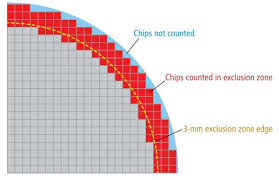
We also have to account for the rectangular footprint of LEDs. They don’t perfectly fit in the round shape of the wafer—some LEDs will be lost by partially crossing into the exclusion zone. In a similar way to the exclusion zone, these losses are a higher percentage of the total for the smaller wafers.
Sources:
LEDs Magazine, “Improve LED manufacturing via in-line monitoring and SPC”, http://www.ledsmagazine.com/articles/print/volume-10/issue-7/features/improve-led-manufacturing-via-in-line-monitoring-and-spc-magazine.html.
LEDs Magazine, “Manufacturing LEDs on large diameter substrates: What’s the hold-up?”, http://www.ledsmagazine.com/articles/print/volume-10/issue-2/features/manufacturing-leds-on-large-diameter-substrates-what-s-the-holdup-magazine.html.
Photo credit: http://www.ledsmagazine.com/content/dam/leds/migrated/objects/features/10/2/12/ARCFig2.jpg.
----
Janine Hueners
Marketing Specialist
Palomar Technologies, Inc.