Photonic integrated circuits (PIC) have become an attractive platform for data center, sensing and medical devices. Thermal cameras and LIDAR for tomorrow’s semi-autonomous and autonomous vehicles, high power LEDs, photo sensors, 3D sensing, gene sequencing – are all just a few of the applications being developed today using photonics technology. Every day, development of these complex digital technologies continues to grow at a rapid pace, challenging existing technology giants and start-ups alike to keep pace with the growing demands for higher data capacity, faster speed, smaller designs and more sustainable solutions that are the foundation of the connected world.
With today’s rapidly changing technology, time-to-market is one of the most important factors for product success. The ability to rapidly develop and test photonic chip assemblies and then implement fast production ramp-up are key to delivering a quick ROI needed to maintain pace with technological changes. Often times, the cost of equipment, lack of manufacturing expertise. or even the lack of engineering/technical staff can hinder even the best ideas from ever being developed or tested, let alone becoming a commercial product. The economic realities of modern, advanced photonics chip packaging with the capital equipment requirements, clean room needs and labor costs, along with the need for process development and low volume production are hurdles that can be overcome by outsourcing to a photonics packaging contract manufacturer.
Successfully outsourcing photonics chip package R&D, development and production
Outsourcing part or all of the R&D, development or production can be the answer to reduced costs, rapid ROI and meeting time to market demands. The advantages of outsourcing are many:
|
.jpg?width=1281&name=Assembly%20Services%20technician%20(2).jpg) |
The Advantages of Palomar Technologies Assembly Services
Palomar Technologies Assembly Services is a full-service advanced packaging laboratory providing solutions for process development, prototyping, test, and contact assembly services. From die attach to wire bonding through package assembly, test, measurement and even prototyping and process development, Assembly Services can provide everything from a complete 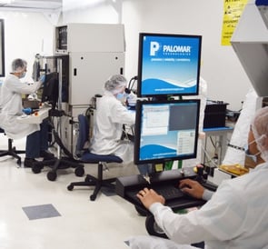 outsourced manufacturing environment to expert prototyping services and process optimization leading to equipment purchase.
Their lab contains Palomar Technologies' high-accuracy, large work area and high reliability automated wire and die bonders including the new 6532HP, SST Vacuum Reflow Systems' high reliability vacuum reflow ovens, precision dispensers from GPD Global, state-of-the-art test and measurement equipment from Nikon, Keyence, XYZTEC, and robust plasma cleaning technology from March. In addition, they offer complete intellectual property (IP) protection.
With over 40 years of experience in the industry assembling microelectronic and photonic chip packages, their highly skilled in-house engineering staff and technicians remain close to Palomar Technologies design and manufacturing engineers, providing a close feedback loop and reducing any downtime. If you need rapid prototyping to small production runs (1000’s units per week), contact Palomar Technologies Innovation Center.
Download the Innovation Center Brochure for more information:
----
David Rasmussen
General Manager, Palomar Technology Assembly Services
Palomar Technologies, Inc.