The International Wafer-Level Packaging Conference (IWLPC) was held in San Jose, California in October. Over 650 industry experts were in attendance, with 65 companies exhibiting. Two of the primary areas of focus were 3D IC packaging and MEMS packaging.
Focusing on automated die attach, Palomar Technologies and SST International shared solutions for wafer-level packaging for both 3D IC packaging and various MEMS packaging concepts. A number of processes can be applied when addressing these packaging needs. By far, the vast majority of methods include eutectic die attach and conductive and non-conductive epoxy die attach.
Eutectic Die Attach
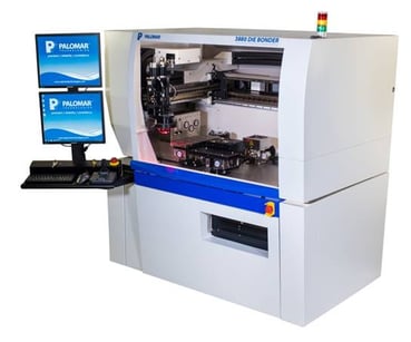
Eutectic methods span the much cooler processing soft solders (most lead free) to the hard solders such as gold-tin (AuSn) and gold-silicon (AuSi). Palomar’s new 3880 Die Bonder has the positional precision and accurate temperature control and monitoring to provide very robust, near void-free die bonds. Need even less voiding? Look to SST’s solutions, including their Model 5100 Vacuum Pressure Furnace.
 |
 |
Pulsed Heat/Steady State Technology
With 0.1 micron encoders, the 3880 Die Bonder can get the die--flipped or traditional face up--to the right location with near 3 micron, 3 sigma repeatability. Once we are where we need to go, we can process solders with either pulse heat technologies or the more traditional steady state methods. Temperatures from ambient to 450°C or more are available in both modes.
When we evoke the highest accuracy process (pulse heating), we also automatically monitor actual temperature profiles of the process, making certain that we provide the right recipe each and every time we go through the profile. If an upper or lower spec limit is hit or exceeded, our bonders stop, log, and present the issues to the operator or process engineer. Since we are holding the die or package during this reflow process, we attain maximum Final Placement Accuracy (FPA). The 3880 is rated at 5 micron, 3 sigma FPA given reasonable materials.
Stacked Die
| Complex vision algorithms allow the 3880 to apply the proper methods for stacking die and other materials such as lenses, rotators, VCSELS, MEMS, and edge-emitting laser diodes. The active optical cable market is expanding very rapidly and the 3880 has a wide variety of solutions for all of this market’s needs. |  |
Non-Conductive Epoxies
In some cases, optical elements or even active integrated circuits require high-accuracy placement with non-conductive epoxies. There is a new group of non-conductive materials available today that can be snap-cured with UV activation. The 3880 Die Bonder can provide maximum Final Placement Accuracy and force the UV activation in-sutu while holding the device, much like pulse heated eutectic applications. Many times these products are still baked out with convection ovens to drive off any leftover volatiles that are not wanted in the package prior to lidding.
Conclusion
The 3D and MEMS packaging space has been growing for years. There are now entire groups of professionals working on these specific technologies and they will grow rapidly in the future. Palomar Technologies and SST International will continue to generate new solutions to this complex space as we move forward with new and even more powerful packaging processes.
Please join us at the dozens of technical conferences that we exhibit at and attend worldwide each year.
Download these resources for more information:
| 3880 Die Bonder Data Sheet |
Pulsed Heat Stage eBook |
SST International 5100 Data Sheet |
 |
 |
 |
| Epoxy Die Attach eBook |
Eutectic Die Attach eBook | Pulsed Heat Stage Data Sheet |
 |
 |
 |
-------------
Bradley Benton
Regional Account Manager, Western Americas
Palomar Technologies, Inc.