Carlsbad, CA – August 23, 2022 – Palomar Technologies, a global leader in delivering total process solutions for advanced photonics and microelectronic device packaging, announced today that Bay Photonics, an advanced photonics assembly and packaging company has taken delivery of a Palomar 9000 Wedge Bonder as a requirement for meeting the demands for wedge-to-wedge bonding by their customers.
“Over the past years, we’ve needed to migrate away from older technology platforms and the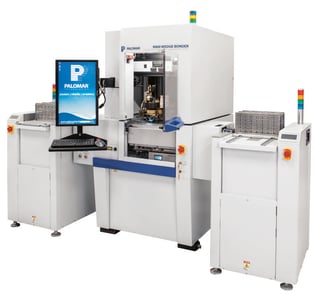 Palomar 9000 offers us a machine with better performance and reliability that is capable of high-volume throughput,” said Glenn George, CEO of Bay Photonics. “We’re placing the 9000 in our laboratories within the EPIC-Center, which along with a range of other Palomar machines, enables us to satisfy some of our more stringent customer needs. Plus, this gives them the confidence that their device has been designed for manufacture.”
Bay Photonics will initially use the 9000 Wedge Bonder for several advanced photonics applications, including unique secure space communications technologies, along with high-end nuclear power station solutions. Wedge bonding enables bonding with a large variety of wire and ribbon materials, such as gold and aluminum enabling thermosonic and ambient processes, which makes wedge bonding an ideal bonding choice for high-mix environments.
The Palomar 9000 Wedge Bonder is a high-speed fine wire and ribbon wedge bonder driven by voice-coil technology in the bond head. This machine has interchangeable 45-60° and 90° deep access wire feed and wedge clamp options and operates across a single large 304 x 152 mm work area. As the entire bond head mechanism rides on a theta axis, users can take advantage of excellent wire tension, a shorter wire feed path and inherent prevention of twisting of wire and ribbon, and better overall process control.
It’s frequently used for these opto-electronic/photonics applications:
- Deep Access Packages
- Constrained Access Package Walls
- High Bit Rate Modulators
- Optical Transceivers
Other applications that the Palomar 9000 Wedge Bonder is used for include:
- RF-SOE
- Disk drives
- Large complex hybrids
- COB
- RF and microwave devices
- Compact hybrids
- Fine pitch devices
- Low profile wire bonds
- Ribbon bonding
- MCM power connections
About Palomar Technologies
Palomar Technologies makes the connected world possible by delivering a Total Process Solution™ for advanced photonic and microelectronic device assembly processes utilized in today’s smart, connected devices. With a focus on flexibility, speed and accuracy, Palomar’s Total Process Solution includes Palomar die bonders, Palomar wire and wedge bonders, SST vacuum reflow systems, along with Innovation Centers for outsourced manufacturing and assembly, and Customer Support services, that together deliver improved quality and yield, reduced assembly times, and rapid ROI.
With its deep industry expertise, Palomar equips customers to become leaders in the development of complex, digital technologies that are the foundation of the connected world and the transmission of data generated by billions of connected devices. Palomar solutions are utilized by the world’s leading companies providing solutions for datacom, 5G, electric vehicle power modules, autonomous vehicles/LiDAR, enhanced mobile broadband, Internet of Things, SMART technology, and mission-critical services.
Headquartered in Carlsbad, California, Palomar offers global sales, service and application support from its offices in the USA, Germany, Singapore, and China. For more information, visit: http://www.palomartechnologies.com
About Bay Photonics
Bay Photonics are an independent Photonics IC (PIC) assembly and packaging company. Helping innovative projects from the research/bread board stage through to volume production. Academic and commercial projects accepted.
They specialize in helping build prototypes that require a flexible and technically innovative approach to package design, assembly and test of devices. Designs requiring single fibre(s), fibre arrays and micro-optics are our specialty. Having worked at world leading opt-electronic component manufacturers, our technical team have vast experience in developing the right packaging and production solution for PICs in various applications including datacom, quantum and medical amongst others.
Located in the South West of the UK, with our main office in Paignton at the Electronics & Photonics Innovation Centre (EPIC), we are housed with other members of the Torbay Photonics Cluster ecosystem and together, offer extended expertise and capability. www.bayphotonics.com, email: info@bayphotonics.com
###
Media Contact:
Rebecca Janzon
Director of Marketing Communications
Email: rjanzon@bonders.com
Mobile: 760-409-7453