Carlsbad, CA – July 19, 2022 – Palomar Technologies, a global leader in delivering total process solutions for advanced photonics and microelectronic device packaging, announced today the expansion of its Innovation Center in Singapore to meet a growing demand in Southeast Asia for process development and specialty OSAT for advance semiconductor new product introductions.
Palomar opened its Innovation Center – Singapore in November of 2018 to address a vital market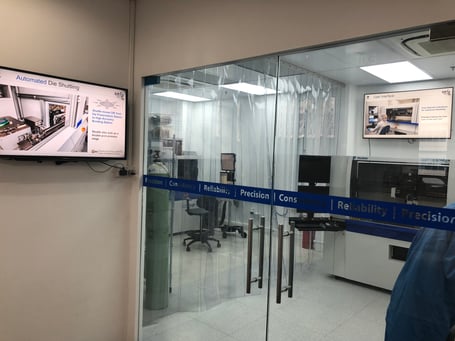 need for process development, device package prototyping, test and measurement, process maturation and low-volume production. In 2019, market demand pushed Palomar to make its first expansion. This second expansion gives the center the added ability to work closer with customers on their specific needs.
“Strong demand from our regional Asia Pacific customer base has driven us to expand the footprint of our Singapore Innovation Center for the second time in five years,” said Rich Hueners, Managing Director, Palomar Technologies (SE Asia) Pte Ltd. “This expanded area will serve to host plasma cleaning, dry boxes and customer-specific test equipment while the original lab area will continue to host the die attach, wire bond and vacuum reflow equipment. We are looking forward to forging ahead with new customer requirements in this larger space.”
The Palomar Innovation Center – Singapore currently supports a wide range of customer applications including:
- Micro optics used in 3D Imaging, LIDAR and Optical Sensors
- RF LDMOS and RF GaN power amplifiers
- High-reliability RF Microwave modules
- Silicon Photonics and laser diode placement bonding
- Thermal and Motion Sensors
- Optical transceiver packaging
- Active Optical Cable packaging
- VCSEL, EEL, EML, LED placement and bonding
- Lens placement and lens attach bonding
About Palomar Technologies
Palomar Technologies makes the connected world possible by delivering a Total Process Solution™ for advanced photonic and microelectronic device assembly processes utilized in today’s smart, connected devices. With a focus on flexibility, speed and accuracy, Palomar’s Total Process Solution includes Palomar die bonders, Palomar wire and wedge bonders, SST vacuum reflow systems, along with Innovation Centers for outsourced manufacturing and assembly, and Customer Support services, that together deliver improved quality and yield, reduced assembly times, and rapid ROI.
With its deep industry expertise, Palomar equips customers to become leaders in the development of complex, digital technologies that are the foundation of the connected world and the transmission of data generated by billions of connected devices. Palomar solutions are utilized by the world’s leading companies providing solutions for datacom, 5G, electric vehicle power modules, autonomous vehicles/LiDAR, enhanced mobile broadband, Internet of Things, SMART technology, and mission-critical services.
Headquartered in Carlsbad, California, Palomar offers global sales, service and application support from its offices in the USA, Germany, Singapore, and China. For more information, visit: http://www.palomartechnologies.com
###
Media Contact:
Rebecca Janzon
Director of Marketing Communications
Email: rjanzon@bonders.com
Mobile: 760-409-7453