Series of three webinars offering insights into prototyping through volume production
Carlsbad, CA – January 19, 2021 – Palomar Technologies, a global leader in delivering total process solutions for advanced photonics and microelectronic device packaging, announced today a series of three webinars designed to present and discuss the challenges of manufacturing and process development for semiconductor packaging. The series focuses on the difficulties start-up companies and independent divisions can face during the journey from package prototype to full-scale production.
The journey from concept to full-scale semiconductor packaging is often hindered by a number of different obstacles along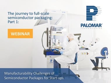 the way including everything from diverse teams scattered across the world to simply not understanding how the manufacturing process of die bonding, wire bonding or vacuum reflow impacts the package design. In this 3-part series, Palomar Innovation Center Engineering Manager, Nicholas Evans and Palomar Product Marketing Manager, Kyle Schaefer present the challenges faced when moving from package design and prototyping, through process development and process optimization to ensure the device can indeed be manufactured with the desired throughput and quality.
In Part One, they will present the challenges of manufacturing semiconductor packaging that many small, start-up companies may face. Often, start-up companies or divisions of larger companies may not have a complete team available and might not be aware of how to take their package from design to full-scale production. In the following two parts, they will present the challenges of optimizing the manufacturing process, as well as the advantages of out-sourcing process optimization to improve time to market.
Attendees can register for the first part of the 3-part series here: https://attendee.gotowebinar.com/register/1391725945623282447.
About Palomar Technologies
Palomar Technologies makes the connected world possible by delivering a Total Process Solution™ for advanced photonic and microelectronic device assembly processes utilized in today’s smart, connected devices. With a focus on flexibility, speed and accuracy, Palomar’s Total Process Solution includes Palomar die bonders, Palomar wire and wedge bonders, SST vacuum reflow systems, along with Innovation Centers for outsourced manufacturing and assembly, and Customer Support services, that together deliver improved quality and yield, reduced assembly times, and rapid ROI.
With its deep industry expertise, Palomar equips customers to become leaders in the development of complex, digital technologies that are the foundation of the connected world and the transmission of data generated by billions of connected devices. Palomar solutions are utilized by the world’s leading companies providing solutions for datacom, 5G, electric vehicle power modules, autonomous vehicles/LiDAR, enhanced mobile broadband, Internet of Things, SMART technology, and mission-critical services.
Headquartered in Carlsbad, California, Palomar offers global sales, service and application support from its offices in the USA, Germany, Singapore, and China. For more information, visit: http://www.palomartechnologies.com.
###
Media Contact:
Rebecca Janzon
Director of Marketing Communications
Email: rjanzon@bonders.com
Mobile: 760-409-7453