Carlsbad, CA – September 18, 2018 – Palomar Technologies, a global leader in total process solutions for advanced photonics and microelectronic device packaging, announced it is enlarging its engineering laboratory to meet the increased demands of customers developing advanced photonics solutions, such as LiDAR, 3D sensors, gene sequencing and high power LEDs. The upgraded laboratory will be used to further strengthen Palomar’s focus on partnering with customers, giving them insight into, and an opportunity to contribute to, Palomar’s technology road map and development of the next generation of systems and assembly solutions.
“Palomar has a long history of partnering with our customers to provide them with advanced solutions for microelectronic and photonic chip assembly and packaging,” said A.J Wilson, CMO for Palomar Technologies. “The explosion of IoT and the connected world has pushed the need for devices with higher data capacity, faster speed, smaller designs and more sustainable solutions. Our upgraded engineering lab provides customers the opportunity to work closely with Palomar in the development of our next generation systems designed to meet the stringent placement accuracy requirements for optimal optical couplings.”
Palomar recently launched the 6532HP 1.0 μm placement accuracy die bonder, specifically designed to meet the rigorous demands for manufacturing photonics devices. Designed to provide high precision, high production and high performance, the new system extends Palomar’s design philosophy for flexibility and offers a variety of options for customization and optimization to meet customers’ requirements. Its introduction has been well received and with the extended engineering lab, Palomar is working closely with customers to enhance the productivity and accuracy of this system even further.
Upcoming Events
Palomar Technologies is exhibiting at the 44th European Conference on Optical Communication (Booth #677) in Rome, Italy from September 24-26, 2018 and the iMAPS 51st International Symposium on Microelectronics (Booth #503) in Pasadena, CA, USA from October 8-11, 2018.
About Palomar Technologies
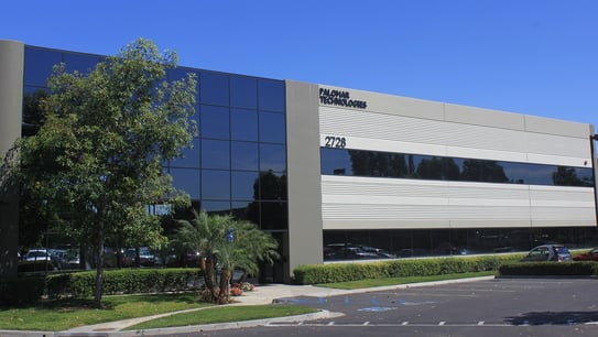
Palomar Technologies is a global leader of automated high-accuracy, large work area die attach and wire and wedge bond equipment and precision contract assembly services. Customers utilize the products, services and solutions from Palomar Technologies to meet their needs for microelectronic and photonic packaging, complex hybrid assembly and micron-level component attachment. For more information, visit: www.palomartechnologies.com.
###
Media Contact:
Rebecca Janzon
Director of Marketing Communications
Email: rjanzon@bonders.com
Mobile: 760-409-7453