Palomar Innovation Centers are experts in process development and work with customers in the areas of design for manufacture, process development and optimization. This case study documents an example of a customer made a design change that altered the functionality, but did not pay attention to manufacturability. The design change resulted in un-bondable pads and all of the prototype materials could not be used to generate builds for testing and validation.
The case study one offers an overview of an unintended consequence of a design change. The device was a custom MEMs die in an emerging technology field and was at the beginning phase of conceptualization and proof of concept. The focus during this phase was the device performance in the early design and not on the packaging or the final performance of the product.
The first revision of the device included wire bonding. While the metallization of the part allowed for successful wire bonding, the device itself did not meet the desired performance metrics. The MEMS die was then redesigned to improve performance. However, during the redesign process, changes were made to the die’s wire bond pads making them no longer wire bondable.
Figure 1 is an example where the appropriate care was not spent on the wire bond metal stack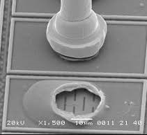 up, therefore resulting in cratering or bond pad lifting which is seen in the lower part of this image. This cratering/delamination of the bond pad can be caused by combination of poor metallization on the device coupled with the ultrasonic action from the wire bonder.
An immediate solution to this problem was to use moly tabs, also called wire bond tabs, as intermediary surfaces to bond on and to overcome some of these issues. Moly tabs are typically used at the board level of a PC board if the surrounding SMT components are over reflowed and the solder migrates to where the wire bonding is to happen. This makes it impossible to bond to industry specifications because it is not possible to wire bond on top of solder.
The Moly tabs were bonded directly on top of the wire bond pad with electrically conductive epoxy. This allowed for the circuit to be maintained, while also providing an ideal surface for the wire bonds to be bonded onto. This provided a short-term solution for the customer to keep testing the functionality of the parts, as well as provided feedback for improvements for the long-term device improvements.
.png?width=1400&name=Case%20Study%20The%20Unintended%20Consequences%20of%20a%20Design%20Change(2).png)
Figure 2. Graphic highlighting the primary benefits resulting in greater return on investment for this case study.
The benefit to the customer in this case study was that waste was reduced in this phase of the prototyping build, as well as reduced development time because the devices were useable for this prototyping phase.
For more information, download our article: The Journey to Full-Scale Semiconductor Packaging Manufacturing.
Download these resources for more: