The medical device market is expected to diversify significantly, almost double in value to $90 billion by 2025, but vendors face significant cost and packaging challenges if they are to exploit successfully these opportunities. Increasingly, there is a growing range of technical, commercial, and regulatory demands. As a result, the imperative to find a focused, strategic, commercially cognizant process—with specific-field experts and proven partners to cut through these shifting parameters—is more important than ever.
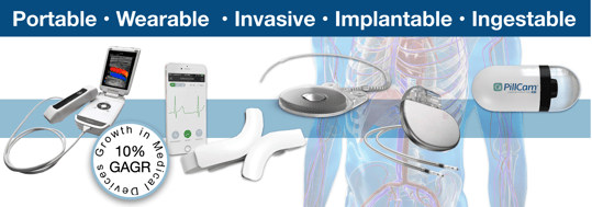
Whether it’s an implantable or wearable device, medical instrumentation, or a life science consumable, there are issues of ever-tightening regulation across a range of jurisdictions, especially for the more invasive products. Technically the interaction of human chemistry with photonic components, as we see in some wearable devices, adds another layer of complexity that must be resolved. Implantable devices must also navigate around the rigors of balancing longevity with performance. Weighing up one against the other is often very difficult, which partly explains the complexity of the issues that must be tackled. Against such often investment-costly dynamics, anything that can improve the financial effectiveness of development and manufacturing is welcomed.
 Small Scale Medical Devices Market Demand 2020-2025
Historically, “latency” describes the time interval between stimulation and response, cause and effect. Contemporary use has considerably widened the terminology to include functional aspects of architecture, capital markets, bandwidth, robotics and more. We use the term in an engineering/commercial sense and more particularly in regards to improving efficiencies in the microelectronic medical packaging process—from concept to full-scale commercial manufacturing. The most critical points of low latency manufacturing are those adopted in the initial stages of process development and prototyping. These tend to take on a life of their own and adopted thoroughly enough have an exponential impact—and value—down the manufacturing process.
Low latency manufacturing is not about approaches to efficiency per se, but (1) where it takes place, (2) people skills and alignment, and (3) the level of customer connectivity. In the biophotonics and medical device ecosystem, additional pressure comes not only from rapidly growing markets and application diversification but also from swift technological advancement and downward pressures on costs. Added to which are the complexities of device approval and certification across a range of jurisdictions. This is true of wearable devices but especially true for implantable medical devices. One must consider that implantable devices are directly dealing with people’s lives, as these devices are not easily replaced or removed. Chip packaging assembly and manufacturing need to be able to deliver a highly repeatable, accurate process.
Medical technologies have been at the forefront of research and development and subsequent commercialization across many ultra-high-tech sectors over the past decade, quickly becoming more advanced and discreet, more portable, less invasive and often more intricate in construction and packaging. This reflects high levels of research and investment, advancing science and their merging to create more sophisticated therapy and diagnostic technologies. Thus, in the past several decades we have moved from cardiac rhythm management products—the pace-maker—to devices that can be used to treat sleep disorders, pain management, certain forms of dementia and related illnesses, epilepsy, bladder control, gastrointestinal disorders, some autoimmune diseases to a range of neurological and psychological disorders. The number of medical devices with computer chips has exploded.
This article presents advanced development protocols drawn from over 40 years of experience that allow Palomar’s Innovation Centers/Assembly Services and their customers to navigate successfully through the factors surrounding medical device packaging. Detailed is Palomar’s strategy to allow fully formed research to move optimally from the first stages of development and prototyping to manufacturing and commercialization. Efficiency born through experience is critical in the concept-to-trial and error stage, thereafter finding important applications moving from technical success to packaging, to full-scale commercialization. At each step-adopted pragmatics are deliberately placed against core commercial demands ranging from the cost premium on innovation to skill shortages to the impact of ever more aggressive competition. In summary, the sustainable medical device market requires a packaging manufacturing culture that is acutely ‘green and lean’, optimized, agile and efficient. This is the essence of low latency manufacturing.
Palomar has over 40 years of expertise in photonics/semiconductor device assembly for high quality/high-reliability industries and Palomar Innovation Centers represent ‘a bridge of ability’ that spans all the way from the original idea to full commercialized production. What has given Palomar a ‘head-start’ in the ‘green and lean’ advantage is our long history of collaboration in packaging development across a spectrum of core technologies; 40 years of experience in LEDs, packaging RF GaN and other processes requiring similar competences.
Palomar’s low latency manufacturing strategy brings together core areas of design, the process approach and, manufacturing. This, in turn, provides feedback, iteration and timely action. The result is not only a better product more efficiently manufactured but also one with higher returns on capital outlay.
| Download the full article: Low Latency Manufacturing for Biophotonic and Medical Packaging: | Download the Innovation Center brochure: |
 |
 |
----
Anthony O’Sullivan
B.Sc, M.Phil, Ph.D., Strategic Market Analyst