This blog is a snippet of larger technical paper, due for release in Q4 2019, written on the topic of eco-sustainability for packaging of power devices using pressure-less Ag sintering methods. Here we will share some of our initial findings and analysis.
Silver Sintering technology has been around since the 1980s, but has recently gained more attention and found increased utility due to innovations in nano-particle materials, greater emphasis on energy and eco-sustainability and wider adoption of lead-free legislation across the world. This article will discuss the work that Palomar has undertaken to demonstrate sustainable packaging and assembly die attach using pressure-less silver sintering die attach for high temperature (>300’C) power electronics.
Long before we performed our work, much research and development has gone into finding a reliable and sustainable die attach method that could replace or at least augment eutectic soldering for power electronics. The two leading approaches for consideration on this topic for high temperature (300’C) power electronics are:
- Pressure silver sintering
- Pressure-less silver sintering / Ag sintering
We will focus on pressure-less Ag sintering and for reasons which we will go into greater detail on later, as the choice alternative for a sustainable and cost-effective lead-free process due of its compatibility with current day manufacturing processes and its potential for being a drop-in solution, most specifically for RF GaN power amplifier packaging.
Choice Alloy: Silver
Silver is an excellent alloy for high temperature power electronics. Silver is considered very viable for three reasons:
- Silver has excellent thermal and electrical performance
- Silver is a lower cost material vs. gold
- Silver has low temperature sintering capability
Pressure-less Ag Sintering
There are several advantages to pressure-less Ag sintering for die attach which are inherent to the material and process themselves:
- Silver can be sintered in the presence of air.
- Silver can be dispensed using the same set of tools and with a similar process as solder paste.
- Pressure-less Ag Sintering does not require special tooling to avoid damaging the die, as required in conventional pressure (240’C temp + MHp XX pressure) Ag sintering.
- Ag Sinter paste uses nano-particles that increase the surface area coverage. This has the effect of making the material more prone to sintering, and doing so without pressure. The further science behind this is that smaller particles have more free energy and need less external energy to initiate the fusion process.
- Current Ag sintering (pressure-less) materials allow for coverage of these larger surface area die whilst maintaining low porosity. Ag Sintering had the previous disadvantage of not being able to cover the surface area of larger dies due to the makeup of the material, but innovations in material make this disadvantage no longer a factor.
Case Study – Snapshot
In our case study, we looked at the problems faced in die attach processes for power electronics and specifically in RF GaN power amplifiers. The solutions developed and of which this paper documents are the following:
- Demonstration of the creation of a fixed height bond line with the Ag sinter paste in an automatic, high speed, highly repeatable process which is also virtually void free.
- Assurance the Ag sinter paste does not shift or move the die after placement so as to maintain planarity for the downstream wire bond process.
We achieved a void-free Ag sintered bond line where there is total coverage under the die and the Ag sinter material doesn’t creep to the top of the die. Depending on the power rating of the device and the amount of Ag in the Sintering paste, a desired final dry bond line thickness of 30 um typically requires a dry bond thickness of 50 um. To control bond line thickness, engineers will often use physical limiters, such as process tooling and jigs. If an application’s design can tolerate it, designed in mechanical features, including surface finishing techniques and other part geometries, may enable bond line control. One common method is designing a customized pickup/bonding tool that has a taller side wall (the size of bond line thickness to be controlled).
Sometimes the physical characteristics of the adhesive, such as compressibility and its thixotropic properties, particularly if the parts are small and have little mass, will control bond thickness.
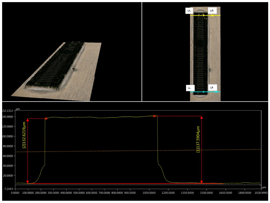 Caption: This image shows the consistency of the bond line and control of the material.
The above approaches have proven to be less than satisfactory in terms of voiding, BLT height repeatability and automation and therefore not a solution Palomar recommends. Knowing the drawbacks of these two BLT control methods, we developed a different solution that is software-driven and has minimal touch requirements. We call this “Fixed BLT." We will demonstrate that this technique and it supporting tools are a very robust solution. The final paper will document our results with a Fixed BLT process in a real RF power electronic application. Read more about our solution.
Blog by:
Redzuan Zin
Applications & Innovation Supervisor, Palomar Technologies South East Asia
Rich Hueners
Vice President of Sales and Managing Director of Palomar Technologies South East Asia
Learn More: