While Engineers can get mildly enthusiastic about what the rest of the semiconductor industry perceives as unduly narrow areas of technology, they rarely use one superlative, let alone several in one paragraph.
If for no other reason than this historic temperance, the extravagant language currently being adopted to describe the arrival and impact of chiplet technology ought to make us sit up and take note. Even interpreting such loquacious vocabulary with a large grain of salt, we ought to prepare ourselves for potentially tectonic changes in the way we approach semiconductor packaging. Most especially in the way we approach advanced design, prototyping, development and manufacture.
While both the nature of chiplet technology, and the drivers of change, have been noted in a previous blog, the key elements are worth restating. Especially because they are so succinct, their impact straight forward to grasp, and they so clearly explain why there is a sudden rush to be on-board; namely, the global race to develop artificial intelligence (AI) and the global need to reach carbon neutrality by 2050.
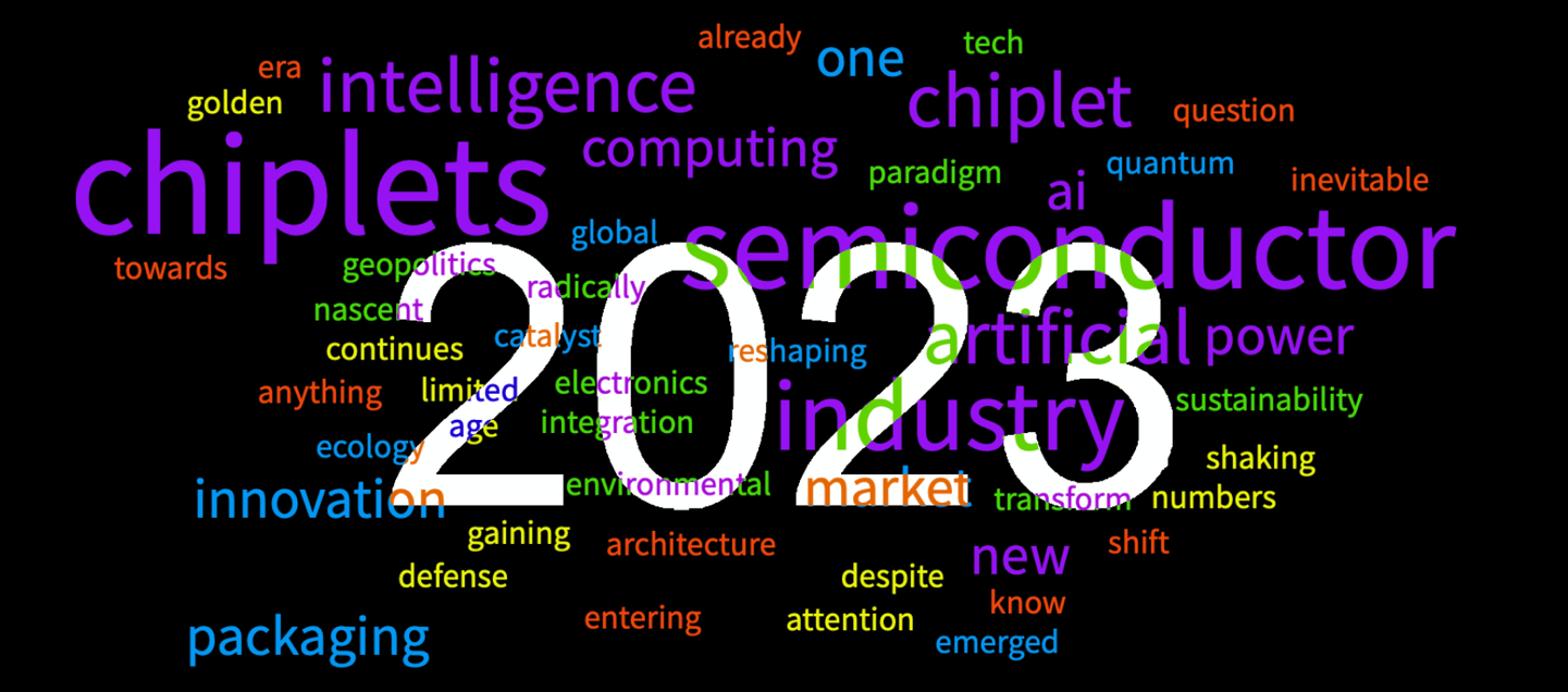
Though chiplet technology has taken more than a few years to get to this point, 2023 may well be viewed by historians as the moment in which all the critical players lined up behind the idea, as they now are. Across the globe the semiconductor industry has come together to develop a common interface and other necessary elements of standardization. Some of them have joined out of the blue, which is one aspect of what has made the past twelve months so momentous.
Another aspect worth mentioning is how widespread the “Lego” analogy has become. Lego so well captures the extraordinary versatility of the technology, limited only, as with the toy, by the constraints of imagination; a degree of hyperbole maybe, but a lot closer to the truth than less expansive interpretations. Indeed, at this juncture we touch on the enigmatic reality at the heart of the overall excitement. As the semiconductor industry successfully advances the capabilities of artificial intelligence and machine learning, the intelligence so created has greater and greater input into developing the next generation of device, and so on. All this we hope to be a virtuous—not ominous—circle of advance.
Most readers will be aware of the very public concerns over the speed at which AI is advancing; the potential, just outlined, marking one of the most important of these. It may be very difficult to fathom, but the high probability that AI could surpass the sum all human intelligence by mid-century is just that, highly probable. While it is vital to understand that this intelligence is very different from human intelligence, from an interface point of view, it will be impossible to tell the difference. This is the ultimate point of concern. It is challenging to discern whether the current solution of creating an AI to police AI is of comfort, or just adds to the overall potential worry. Notwithstanding, AI will unleash a tsunami of creativity, not least, as we have implied, in furthering new approaches to new forms of packaging.
Rather less enigmatic is the fact that as AI advances the value of the simulation protocols it offers grows commensurately. This has the potential to reduce the cost and speed up the process of new design and development. Time will be saved and physical waste reduced considerably. Equally, by so accurately mimicking the properties of meta-materials, new epoxies, new forms of thermal management, and so on, simulation will both quicken and improve outcomes while spending less. Any temptation to Luddism on the part of Mechanical and Electrical Engineers, however, should be resisted. In terms of the absolute number of new opportunities to physically build and prototype these will still grow considerably—more than making up for the practical impact of advanced simulation.
Another reason for anticipating 2024 as the beginning a new era for the semiconductor industry, is that the packaging evolutions which have proven key enablers for chiplets, are now themselves moving towards growth and maturity. Most especially we reference 2.5 and 3D packaging and hybrid bonding. These technologies are absolutely essential to advanced chiplet manufacture. Though we have spoken of “suddenness” and “surprise”, this has been no surprise to those thoroughly engaged in the direction of the semiconductor industry. A review of new entrants to the die and wire bonding ecosystem since 2012, and since 2017 especially, show that they have all the while been targeting these very markets. Additionally, not a few are focusing on specially designed systems for research, development and low-run production anticipating that chiplets will be particular boon to this sector.
No doubt the reader will have swiftly identified the impact of these various developments, and the potential flood of new opportunities for ecosystem participants (including those currently at the margins), and SMEs in particular. Indeed, SMEs may play a much greater role in the advance of chiplet based semiconductor technologies than a number of the mega-companies. This is because many, if not all of these smaller companies, are driven by innovators who really understand their field of expertise, and can take it forward in a singular manner not possible in larger companies. They also have “skin in the game” which translates into effort, energy, focus and a fierce determination to succeed.
Over the years Palomar has worked with a number of such businesses. Their presence initially was barely a blip in the market-place when they began, but today their technology dominates and, in some cases, represents a key enabler to developments in other sectors. As we end 2023 and enter 2024, our engineers both in assembly services and applications look forward to working on many new projects supporting chiplets and other advanced packaging—however many—or few—superlatives characterize their day-to-day conversation! We of course hope you are one of them, but either way, we would like to take this opportunity to wish you a very happy and enjoyable holiday season and technically exciting 2024.
----
Dr. Anthony O'Sullivan
Strategic Market Research Specialist
Palomar Technologies