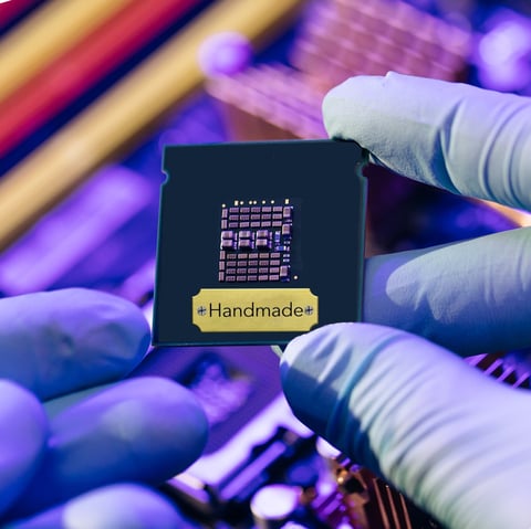
Yes, we still need to do some things by hand. Such is our collective way at looking at the world, that most of us cannot imagine, that when it comes to invention and innovation, the approaches taken in proof-of-concept, prototyping and development, and even early-stage production, these protocols are a lot closer to the Industrial Revolution of the 18th century, than any fanciful process we might see in some set-far-in-the-future, science-fiction movie. The truth is, in the world of automated chip and semiconductor manufacturing, a lot more is done by hand than most people realize, except of course, those who are part of the process. As our opening caption puts it, there is as much relating to semiconductor production and development, past and future, that is handmade.
That being said, if the realm of science fiction is invading anywhere, it is in the realm of artificial intelligence—in the sense of generative AI telling us what we can do with those hands, ideas that we have not remotely considered left to our own unaided devices. This blog proceeds by examining this fascinating tension, as well as giving the reader a clear idea of how this subject may be of practical benefit; either bringing inventor ideas to life, or providing a more grounded solution than existing mind-sets may allow.
At first consideration, much of this hands-on work appears both unglamorous and the unlikely beginning of anything sustainable, let alone exciting, but then even an epic world-tour begins in the surroundings of the familiar and mundane. Which happens to be a great metaphor here. Printed circuit boards (PCB) generally place components utilizing surface-mount technology (SMT) but those embracing high-reliability application designs and higher functional integration mix through-hole (THT) and surface mount technologies (SMT). These hybrid approaches are needed in the arenas of energy (carbon and green) aerospace, defense and security, but especially research and development. In all these cases demand for THT not only remains strong, but is evolving and growing to meet new needs and challenges.
For the more complex THT work, such as the mixed type with SMT, the skill-sets required of engineers/technicians can be demanding, the tooling required, comprehensive and expensive, with testing and metrics generously funded so that the equipment used meets the most exacting standards. The professionals’ journey to this level of competence involves a lot more than simply utilizing time and experience to develop hand-eye-skill accuracy. Beginning with a thorough but practicable understanding of the basics, the next steps continue with the acquisition of a knowledge bank that embraces a thorough understanding of physics, chemistry, design and planning.
As the underlying principles are understood in each of these domains, collectively they create intuitive perceptions that combine what is seen, with what is quickly understood. These engineers develop multi-disciplinary approach to considerations of heat, color, solder types, quantities and contact times, surface characteristics, indicators of contamination, oxidation and contamination type, tools and handling, component placement order, shadowing (the potential impact on the soldering process of placing different sized discrete components next to each other) and thermal imbalance, which can undermine particular components or weaken the overall structure, and, which is a particular challenge with regard mixed SMT/THT assembly.
One thing we have not mentioned are the holes. The reader may reasonably think that holes are so basic to the essence of THT, that there is not much to be said. Certainly, that they in no remote way represent a significant challenge needing thoughtful negotiation. Yet, they do. The size, shape and position of the hole impacts hole fill, which in turn directly affects the manufacturability and robustness of the THT-soldering process, which in turn affects the mechanical reliability and fatigue resistance of a solder joint as well as its current carrying capacity and high frequency behavior. Solder hole fill is difficult to achieve, especially when automated in say a selective wave-flow process, which is why much is still done by hand. There are automated work arounds, but these have to accept the risk of thermal damage to the PCB.
As the distance between pin, hole, and printed circuit board (PCB) thickness can be determined numerically, the challenges of hole dimension can be solved. Other implications pertaining to key physical properties, cannot, however. These include fluid mechanics, heat transfer, and surface tension, which defy such straight-forward solutions, and, in the end, can only be resolved through experience, in other words, trial and error. The current nature of these issues is nowhere made clearer than in the number of publications and type of literature dealing with these challenges. For us at Palomar, our Assembly Service operations witness the same phenomena on the quantity, but above all, the growing variety of THT solutions we are asked to investigate; all done by hand!
As to generative AI and the impact it will have on future—we have already referenced the potential of algorithms to resolve problems in a new light, and technically negotiate them from new angles. Beyond that it is difficult to be more detailed, since these solutions, by definition, are unknown. What is not unknown, however, is the necessity of those who offer assembly services in these areas, to possess the high-quality tooling, comprehensive testing capabilities, and extensive knowledge bank to apply the answers that advanced compute power will suggest. To contact our assembly services manager, Nick Evans, with an enquiry of your own concerning THT or many other packaging challenges, please click here.
----
Dr. Anthony O'Sullivan
Strategic Market Research Specialist
Palomar Technologies