Power electronics are present in our everyday lives in many applications. High-efficiency lighting, elevators, motor converters, solar energy, welding, industrial frequency converters, pumps, and a variety of other industrial applications that depend on power electronics.
 Figure 1: Industrial applications for power electronics
In fact, power electronics is so predominant in our lives that the market is expected to grow to over $44 billion by 2025/2026.[i]
One of the critical challenges faced in power modules is thermal management. Several semiconductor packaging variants were developed to address specific market/end-use application needs/requirements. Their design concepts were created by the thermo-electrical requirements, reliability, and power output requirements for each application.
Case Study:
The following case study was performed to demonstrate the low void soldering process for typical soldering surfaces inside the power module, where a large size DBC substrate was soldered with preform to Ni pated base plate. By achieving low void soldering results, it is possible to achieve a larger number of thermal cycles, thus extend the life span of the power module.
A study of the soldering process was conducted as part of the SST 8300 Series Automated Vacuum Pressure Soldering System capability demonstration. To demonstrate the low void soldering results, a base plate (Copper with Ni sulfamate plating), with both SAC 305 and Sn95Sb5 solder alloys preforms and a DBC substrate, were used. See the Figure 3.
The study consisted of the following materials:
- Base plate: Copper with Ni sulfamate plating, Concave shape, dimensions 105 x 45 mm.
- Preforms: SAC305 and Sn95Sb5, both 33 x 63 mm, 200 microns thick.
- DBC substrate: (Cu/Al2O3/Cu), 34 x 64 mm.
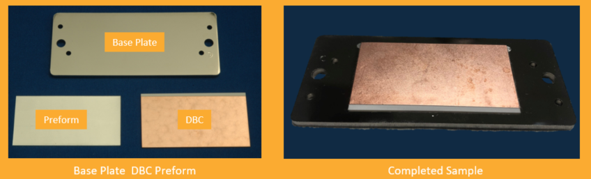
Figure 2: Base plate DBC preform (on the left) and completed sample (on the right)
For this evaluation, graphite tooling was developed to locate the DBC substrate over the Ni plated base plate. Weights were used to apply force on the substrate to ensure good contact with the preform. Five tooling sets were placed inside the 8301 chamber, one in each corner and one in the chamber's center. The intent was to demonstrate the chamber's temperature uniformity and the soldering results repeatability in various parts of the chamber.
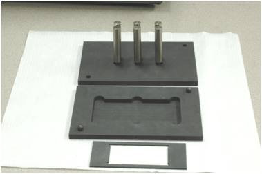 Figure 3: Graphite top plate with free-floating weights, graphite boat to locate the base plate and graphite insert to locate the preform and DBC substrate
The solder alloy's mechanical properties and thickness play a significant role in absorbing the relative motion between the two joined surfaces during the thermal cycles. The ability to achieve low void soldering results using the wide range of solder alloys without flux is one of the critical requirements for modern vacuum reflow ovens.
The SST 8300 utilizes a unique combination of vacuum and gas pressure above atmospheric, to reduce voids close to 1%. This method is ideally suited for large surface areas, such as DBC to base plate soldering.
The chamber within the 8300 utilizes edge-heating elements to enable the chamber to achieve temperature uniformity over the entire thermal process area with a guaranteed temperature uniformity +/-2%.
A typical die attach profile for the 8300 consists of 6 different phases taking the package from a vacuum purge, introduction of Formic Acid, through reflow and eventually cooling, which collapses any voids in the solder.
 Figure 4: Typical die attach profile from the SST 8300 automated vacuum soldering system
Results of Case Study:
Once the reflow process was complete, the void ratio for the solder was checked with the X-Ray inspection. To make the examination easier, the backside of the base plate was milled-out. The typical X-Ray inspection photos for assemblies soldered with both SAC305 solder preform (Figure 6) and Sn95Sb5 (Figure 7) showed void levels are near 1%.
|
|
| Figure 5: X-Ray inspection of SAC305 solder preform showed less than 1% void |
Figure 6: X-Ray inspection of Sn95Sb5 solder alloy show less than 1% void |
Conclusion:
Typical failures in IGBT power modules are often the result of CTE mismatches, which cause thermo-mechanical stresses that lead to solder fatigue and constitutes itself in the form of cracking or delamination. The overheating occurs in the areas of heat transfer (cracks/delaminations), which leads to faster crack propagation. The surface overheating also leads to wire/ribbon bond lifts or heel cracks.
With this case study, it has been demonstrated that using the above method of vacuum reflow utilized in an SST 8300 Series Automated Vacuum Soldering System, it is possible to achieve a very low void soldering result (around 1% on average) while soldering a large DBC substrate to Ni plated base plate with SAC 305 or Sn95Sb5 preforms.
The low void rate mitigates the likelihood of solder fatigue and overheating, reducing failure rates and increasing power module reliability.
To learn more about thermal conductivity and the 6 phases of the SST 8300, download the entire article: Power Module: Typical Failure Modes and How to Solve Them.
Download these additional resources for more information:
| SST 8301 Automated Vacuum Pressure System Brochure | SST 8303 Automated Vacuum Pressure System Brochure |
 |
 |
----
[1] Compiled estimate from various sources.