Towards the beginning of our ABCs of LEDs series, we talked about defects. Here we will tie that in to how defects affect yield of LEDs.
K – Kill ratio
In looking at a defective wafer through an inspection tool, how do you determine which defects are killer defects that impact the yield or electrical performance, and which defects are simply a nuisance? Manufacturers need to detect killer defects at the earliest possible time in terms of the repetitive epitaxial-growth wafer-production runs in an MOCVD (metal organic chemical vapor deposition) reactor.
One approach to separate yield-impacting defects of interest from nuisance is to use what is called kill ratio analysis. Kill ratio represents a proportion of defects estimated to cause die failure. The kill ratio is derived from data gathered over prior production runs and is used to find the amount of defects on a current inspection that will cause die failure at the end of the process.
Given that the kill ratio correlates with defect attributes such as defect size, kill ratio analysis provides important guidance in setting defect attribute binning to identify yield-impacting defects.
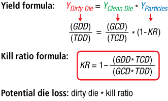
Generally, yield is simply the number of good die divided by the total number of die. In this case, however, we are focused on the yield impact strictly of the die that have at least one instance of the defect of interest, and that leads to the formulas pictured above. In an actual production scenario, manufacturers would perform such an analysis on different types of defects. By binning defect attributes such as defect size and defect location with the kill ratio results, one will finally be able to observe the correlation to yield. In other words, defects with higher kill ratio have more negative impact on the yield.
L – Lattice Match
Epitaxy involves growing a thin crystalline film of one material on top of another crystalline material, such that the crystal lattices match—at least approximately. If the epitaxial film has a different lattice constant from that of the underlying material, the mismatch will result in stress in the thin film.
Conventionally, HB LEDs are manufactured on top of either sapphire or silicon carbide material, because these crystals have a relatively close lattice match with the GaN structures that emit light.

But as the LED industry scales up to meet the twin challenges of cost reduction and more efficient light emission, the use of silicon substrates that can be more easily scaled to larger sizes is seen by many as an obvious way to cut chip costs.
The downside of the GaN-on-silicon method is that the light-emitting structures are based on materials with a poor crystal lattice match – meaning that LED chips fabricated in this way tend to have relatively poor performance.
Sources:
Solid State Technology Journal: “The gleam of well-polished sapphire”, http://electroiq.com/blog/2013/01/the-gleam-of-well-polished-sapphire/.
LEDs Magazine, “Improve LED manufacturing via in-line monitoring and SPC”, http://ledsmagazine.com/features/10/7/10.
Optics.org, “Twin boost for GaN-on-silicon LED ramp”, http://optics.org/news/3/7/46.
Photo credit: http://optics.org/news/3/7/46/PlesseyLED.
http://ledsmagazine.com/features/10/7/10/ledsjul13_mfgeqn.
----
Janine Hueners
Marketing Specialist
Palomar Technologies, Inc.