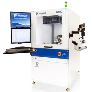
Capital equipment investments are justified on the basis of providing a return on investment. Capital equipment for the semiconductor industry is no different. At Palomar Technologies, we are committed to extending the longevity and maintaining peak performance capabilities for all systems that leave our factory, whether it is a Palomar wire or die bonder or an SST vacuum pressure/reflow oven.

Reach and maintain maximum production value of your semiconductor packaging equipment by implementing these best practices:
- Enroll in a Training Course – To keep production at your bonder’s or vacuum reflow oven’s maximum performance capabilities, take advantage of offered training courses lead by Palomar and SST experts. These courses cover topics like system operations, programming and proper maintenance.
- Maintain a Service Contract – Benefits of service contracts include a number of annual preventative maintenance visits, emergency calls with in-house packaging equipment experts, discounted spare parts, priority shipping of spare parts.
- Upgrade to the Latest Software and Hardware – Outdated software and hardware hinders the ability to run production at maximum capacity and accuracy and may limit our eligibility for field service support.
- Practice Preventative Maintenance for Software – PC Backup and Recover is a safety net for production computer data should there be a program-based data corruption or loss. The PC Backup and Recovery hardware system will reinstall all software and program data to have your equipment up and running in minutes. Compare this with the potential financial losses associated with disrupted production and downtime.
- Hire a Process Development Consultant – Palomar has in-house resources available to develop or optimize production processes on Palomar and SST systems. Our consultants are specially trained engineers with a complete knowledge of equipment, application processes, and material required to increase yield, throughput, and equipment performance.
- Reach out to Palomar with any Questions – Palomar is committed to a strong partnership with your organization and is available to provide applications advice, industry insight, and expertise to improve equipment capabilities.
 Palomar Technologies maintains strategic locations for sales, service and support around the globe to satisfy our customers’ semiconductor packaging needs. Our Innovation Centers, located in Carlsbad, CA and Singapore, along with our prototyping lab in the U.K. provide contract manufacturing capabilities, prototyping and process development consulting.
Download these resources for more information:
| Innovation Center - USA Brochure | Innovation Center - Asia Brochure |
 |
 |