The die bonding, or die attach process, consists of attaching a die/chip to a substrate or package. This attachment can be performed with either eutectic solder or adhesive (epoxy). SST Vacuum Reflow Systems, a Palomar solution recently published an article in Chip Scale Review which discusses the eutectic (where the liquidus and solidus temperature are the same) solder die attach where the preform is an alloy comprising a mixture of two or more dissimilar metals. The preform is a flat sheet of material slightly smaller in area than the die. This preform is typically 25–50µm thick. It is placed between the die and substrate for subsequent melting to wet both the backside of the gold-coated die, and the gold surface of the package/substrate. In our evaluation, the AuSn preform was used with the exact ratio of 80% gold and 20% tin with a melting point of 278°C. This is a critical composition as shown in the phase diagram for AuSn. The inflection point on the phase diagram at the 20% composition of Sn shows the lowest melting temperature of 278°C with much higher melting points on either side of this 20% point.
The equipment used was an SST 5100 pressurized vacuum reflow furnace with highly repeatable control of vacuum, pressure, and temperature. From vacuum levels of below 50mTorr up to positive pressures as high as 40psig, the Windows-based PC system operates automatically to evacuate, pressurize, purge, and exhaust on an incremental time-based cycle. Two or three (optional) selectable gas inputs are available. Process parameters are controlled from software programs running on a Windows-based PC with custom software and off-the-shelf hardware.
Ten devices were provided by the end-user for assembly, where a GaN die needed to be soldered into a AuNi-plated metal ceramic package, with AuSi preform. Custom graphite tooling was fabricated for this evaluation. The graphite boat had a cavity made to precisely locate the metal ceramic package. The graphite insert was fabricated to fit inside the package and provide precise location of the preform and the GaN die.
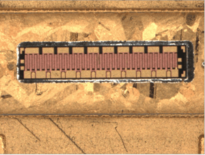 Close up of the soldered GaN die soldered to the package
To ensure good contact between the GaN die and the package, a free-floating weight was used to assure good thermal connection between the die, preform, and the package. The GaN device may be fabricated with or without air bridges. These air bridges cannot tolerate any contact or any force that could collapse or damage them. To protect the top surface of the GaN die, a graphite bezel is placed over the die. The bezel is designed such that its standoffs are contacting the die in safe zones. Therefore, the weight is pressing on the bezel and the bezel is pressing on the die.
The profile started with a combination of nitrogen purges and low vacuum level at room temperature. The next portion of the temperature profile consists of the solder reflow section. This includes the ramp up from the pre-bake temperature to the final programmed reflow temperature, which can typically be from 10 to 50 degrees above the solder alloy melting point.
Once the preform has reached the full liquid state during the heating portion of the reflow, high-pressure (30-50psig) nitrogen gas is introduced into the chamber. This high pressure gas will collapse or reduce the size of trapped voids, and in most cases, eliminate the remaining voids. This technique uses Boyle’s Law (P1V1 = P2V2) to reduce void sizes.
There are four key parameters to control in a vacuum reflow die attach application: 1) ramp-up time, 2) reflow temperature, 3) cool-down time, and 4) total time above liquidus (TAL) [4].
Acceptance criteria are primarily based on either X-ray or scanning acoustic microscope (SAM) scan verification after die attach reflow. A visual appearance of the solder with shiny bright color and excellent fillets is also essential and goes hand in hand with low-void content, as a proof of a well-designed reflow profile.
A successful and robust die attach process is the key to long-term reliability and high performance of a microelectronic device. Proper selection of materials, their plating, solder alloy preform and process parameters of the vacuum reflow process will all have a direct impact on the overall soldering quality (void level). The soldering profile was developed for die attach of GaN die with AuSn preform to a AuNi plated metal ceramic package. The visual inspection of the soldered interface and the X-ray inspection confirmed proper reflow temperature and very low void levels (under 1%). With properly designed graphite tooling and soldering process profile, the consistent low-void results can be achieved in mass production.
Download these resources for more information:
| Achieving less than 1% voiding in GaN die attach processing |
 |
----
Alex Voronel
Director of Global Sales at SST Vacuum Reflow Systems
Palomar Technologies, Inc.
Pierino Zappella
Process Development Engineer with SST Vacuum Reflow Systems
Palomar Technologies, Inc.