The semiconductor packaging industry continues a relentless pursuit to make smaller packages with higher throughput. The industry demand for smaller components requires manufacturers to adapt by developing new processes. Achieving consistent, quality Au Planar bumps has been a challenge that the industry has been trying to meet for years. In this case study, we explore these shrinking specifications of wire bonding requirements in regards to ball bump mashed ball diameter and top heights for flip chip applications and how to achieve them.
The customer presented a specification that demanded a grouping of bonds of 60 micron mashed ball diameter with a top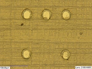 height of 17 microns while targeting a mashed ball height of 15 microns. These bumps would then be bonded on a wafer to be used for flip chip applications. These dimensions are quite difficult to accomplish because the ratio between the diameter and height is so extreme. The required height is considered very low for the desired diameter. Additionally, the top height in relation to the mashed ball height are very close in height and the tolerances are low. Essentially, the customer requested a bump with a planar top. Additionally the groups of bumps should be co-planar.
Achieving the Specifications
In working to meet the customer demands, Palomar looked at three different methods to achieve the specifications for the planar bumps.
- Standard shear motion
- Advanced shear motion
- Two-step coining process
Download the case study to read the results of the three different approaches:
----
Trent Nash
Applications Engineer
Palomar Technologies, Inc.