In less than two decades the RF “family” has witnessed significant growth in the types and varieties of technology served, materials utilized, approaches to packaging, levels of device capability, and the wider synergy of the overall ecosystem. Indeed, it is the latter’s relentless demands for improved power, speed, dependability, scalability and size, that are the key drivers of change, itself triggered by the pull of digitization and anticipation of 5G mmWave and 6G infrastructures.

As in photonics with its pursuit of the homogenous integrated silicon chip, the development of RF GaN technologies has clearly identified ideal endpoints, but like optoelectronics has been “happening” for nearly two decades. Similarly, the passing of the years has only raised the level of skepticism and doubt that commercialization of the next evolutionary goal would ever take place.
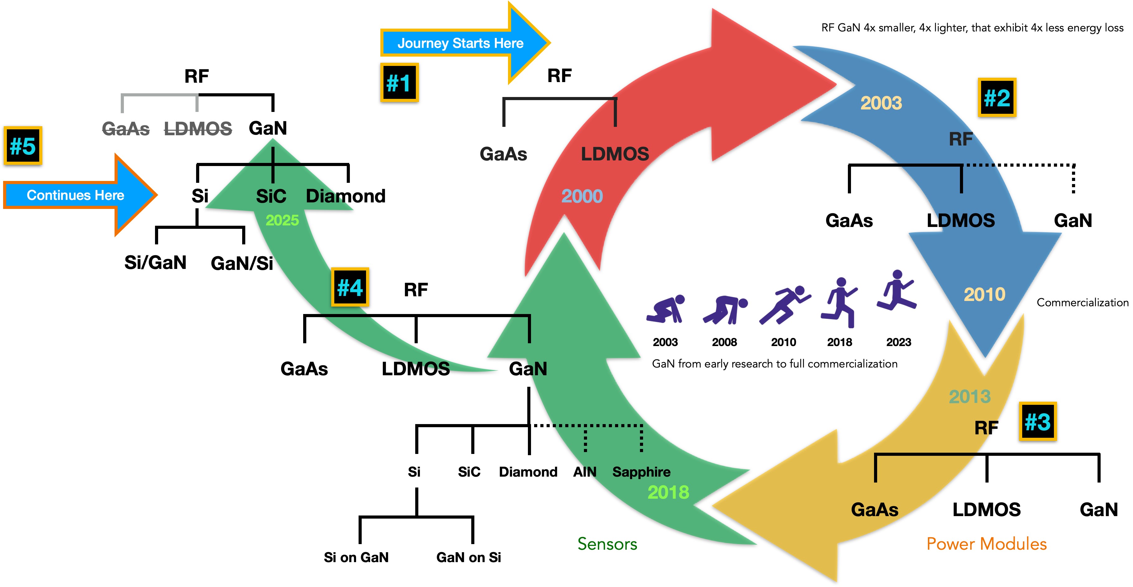
Figure 1. Evolution of RF Technologies 2000-2025.
Notwithstanding, and, as with silicon photonics, commercial production has come and sooner—and with far greater breadth of scope and ambition—than initially anticipated. This is largely due to global operators’ decisions to abandon cheaper LDMOS transistors for higher performing GaN on SiC devices for 5G roll-out, a decision that kick-started GaN adoption elsewhere. So, after years of seeming inertia, we are suddenly there. Before we examine what being “there” means, it is helpful to pause both to review the fundamentals of the technology and also set in place the wider RF evolution which is our context. We begin with the basics.
RF devices are switches that route high frequency signals through transmission paths and are produced in various materials for different applications. As Figure 1 shows, from the early 2000s and for much of the following two decades were dominated by LDMOS (laterally diffused metal oxide semiconductor) and GaAs (gallium arsenide). Beginning around 2003 a third material, GaN (gallium nitride) became a prospect of development interest and exponentially growing investment from industry leaders. The road to commercialization was slow at first, but by 2018 and with 5G and green power then very much on the horizon, GaN was unambiguously the future of RF technology, offering both lower cost and higher performance. Indeed, almost immediately devices were offering a minimum 30 percent more energy efficient, with four times the power density and were up to 90 percent smaller. That, however, is only the starting point in a much longer list of potential advantages that were to be exploited.
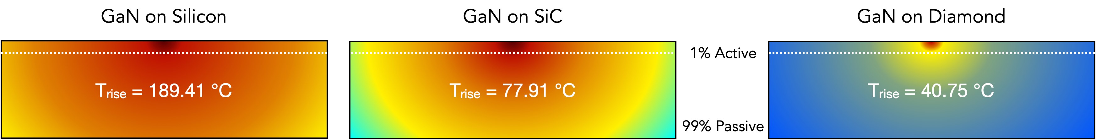
Figure 2. Comparative Thermal Conductivity of 4W Transistors.
The latter were largely predicated on the material chosen to provide the substrate, of which there are three primary and two lesser options; silicon, silicon carbide and diamond, but also sapphire and aluminum nitride. GaN-on-silicon provides for lower performance utilizing low-cost, large-wafer silicon CMOS technologies, and so is perfect for use in price-competitive, high volume manufacturing environments. GaN-on-SiC is the “high-end” version of GaN for RF, coping with the power levels needed by more demanding applications. GaN-on-diamond is the newest approach to packaging RF technologies, and Figure 2 below illustrates in immediate and sharp relief the extraordinary advantage the material offers:
Our representation quickly uncovers the fact that no matter what material comprises the substrate, only the top one percent layer provides the active component, the remaining 99 percent is just passive. It would be a mistake, however, to misnomer “passive” as “largely not doing anything too useful”. Again, as the figure makes immediately clear, nothing could be further from the truth. The issue is one of heat dissipation, which is absolutely critical to current functionalities, and even more so, to the development of a vast range of next generation RF devices. Indeed, thanks to the rising energy costs, material choices may be critical to the commercial sustainability of a large number of current devices.
In short, diamond provides for the highest thermal conductivity of any material, four times that of copper or silicon carbide. This principle alone allows for devices that are six times smaller or achieve six times the power of the current best alternatives, in turn permitting for more compact subsystem or system designs; enable greater system-wide efficiency by dissipating less thermal energy; or delivering previously unachievable levels of power from a power amplifier or unparalleled greater picture resolution from sensors. Packaging requires fewer active elements thereby reducing complexity and system costs but increasing dependability and scalability. Other performance benefits will include the ultra-high data transmission rates essential to the future of 5G mmWave 6G/THz communications, as equally the necessary free-space optic and satellite infrastructures.
As if these were not sufficient motives for rapid development, they have been significantly reinforced by current economic and political stresses, especially the increased realization of the security and defense value of GaN technologies, and their part in realizing super critical competitive advances in the quantum and AI fields. As a result, governments worldwide have significantly increased investment in military and security-use developments.
For these reasons, and unlike the telecom-based photonics boom and bust of the early 2000s, the factors driving this growth in RF GaN technologies have literally trillions of dollars behind them, from global oligopolies to public investment from the world’s largest global economies. In short, both development and manufacturing of future GaN devices is distinctly and decidedly sustainable.
While no longer in its infancy, significant room yet remains for improving GaN-on-diamond performance, scaling potential and integration capabilities. It is in this role that Palomar’s global Innovation Centers continue to play an active role in supporting full scale commercial production of GaN-on-diamond packaging as well as vital continued development work on broader GaN based RF to decrease costs and facilitate integration capabilities across other common processes, but also mapping out of various pathways towards more advanced heterogeneous integration/packaging.
To learn more about the Palomar Innovation Centers around the world, download our brochures:
| Innovation Center – USA | Innovation Center – Singapore |
 |
 |
----
Dr. Anthony O'Sullivan
Strategic Market Research Specialist
Palomar Technologies