Wafer-Level Packaging (WLP) has become widely accepted in the microelectronics industry due to the demand for smaller form factor in portable electronic devices. Added benefits in WLP, when compared to conventional discrete packaging, include:
- Lower cost of manufacturing and testing
- Higher application performance
- Better overall thermal management due to the shorter interconnects
Devices today that have benefited significantly from WLP are microelectromechancial systems (MEMS) and CMOS image sensors. These devices can be found in an array of products from cameras, handsets, netbooks, notebooks, gaming consoles, mobile TV to GPS, Bluetooth, fiber optic communications, and much more.
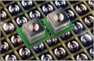 Example of wafer-level camera assembly
According to a recent report by Yole Développement, WLP has been forecasted to exceed 1.7 billion units per year by 2012, at a compound annual growth rate of more than 20% over the next 5 years.
With the trend increasing to move from conventional plastic packages to WLP, assembly challenges had to be resolved quickly to ensure a robust and reliable process could be maintained in high-volume assembly. As many people will attest, process steps developed for prototyping cannot always ensure the same process methodologies can be used when ramping into mid-level to high-volume production.
At Palomar Assembly Services™ (“Assembly Services”), a division of Palomar Technologies, we have developed the equipment and automated processes to support direct AuSn solder bonding of integrated circuits (ICs) onto wafers. This process today is automatically controlled and monitored to provide high-accuracy and precision placement of ICs within 2-3μm to their corresponding silicon circuit on the wafer. This process is preformed on the high-precision 6500 Die Bonder. The 6500 Die Bonder has been designed to provide ultra-high accuracy for eutectic and adhesive die placements.
For eutectic WLP packaging, the product wafer (host) is mounted onto a heated wafer stage. The devices are then picked from either a joining wafer or Gel-Pak™/Wafflepack by a pulse heated pick tool with active cooling and placed precisely within 1.5μm (post-eutectic bond) on the corresponding host wafer. This process allows for tightly controlled and reliable die attach onto the host wafer, resulting in a reliable eutectic bond.
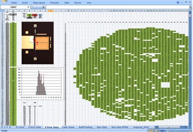
One prime example of Assembly Services’ eutectic WLP assembly is a program involving a 10g Hertz p-side down laser diode used in fiber optic communications. Don Beck, Assembly Services general manager, was at the beginning stages of the program development and commented the following: “With appropriately 3000 die per wafer placements onto 6-inch wafer, the challenge was to meet the customer requirement of demonstrating process consistency. In order to demonstrate a consistent process for WLP, software tools had to be developed to provide real-time statistical monitoring. This software—called Automated Data Management Analysis (ADMA)—was developed internally at Palomar and creates both graphical and numerical analyses of the performance data, allowing for real-time monitoring and analysis through SPC software and component traceability. 100% inspection and SPC was collected at each die placement on the wafer. All data was categorized and stored in time-stamped directories, down to the (ms) for sufficient granularity for both time- and event-based trending of key variables. This maintained a clear picture of process status, which validated the laser diode device placement accuracy onto the wafers.” This validation data is downloaded into a custom certificate of conformance, as shown below.
The 6500 Die Bonder and ADMA software enable Assembly Services to beat the challenges facing many assembly houses today and provide superior manufacturing principles for WLP. Read more examples of how ADMA software has been utilized to increase efficiency and traceability in the lab: Paperless Laboratory: Increased Efficiency and Traceability in Microelectronics Assembly.
----
Julie Adams
Director of WW Sales, Assembly Services
Palomar Technologies