Taking from our last post, we determined that the playing field of contract assembly in complex microelectronics, in regards to cost has been leveled. A primary reason for this "leveling" has been that U.S. manufacturers have proven able to realize the advantages of Designing, Developing a Prototype, Creating a Process, and Manufacturing a Complex Product on-shore and doing it at High-Volume in a cost-effective manner.
What are North America's Advantages?
Let's unpack what some of the advantages of doing contract assembly for mircoelectronic and optoelectronic products on-shore (North America) are:
1) High skill set available for microelectronics design, prototyping, and packaging
2) Intellectual Property (IP) protection
3) Time shortened between prototype and high volume production - freeing up valuable engineering sources sooner and resulting in a quicker time-to-market
4) Allows Managers and Sr. Engineering staff to react to changes or problems much more effectively
5) With the above-stated advantages, the contract assembly firm's ability to perform consistent complex applications and processes is strengthened
7) Close to many end users - again reducing time-to-market and enabling greater flexibility to make quick changes if needed to match market needs
Automation in Microelectronic Manufacturing
Time is money; automation cuts time down dramatically; automation is more cost-effective. When automating a complex process, setting up the process correctly the first time becomes imperative aspect in determining whether or not you will reach your time-to-market goals. A glaring benefit of automation is that an operator or technician can run a complex process (an operator or technician is cheaper than an engineer, obviously). But as with anything in life or business, things can go wrong, even in automation and even with a picture-perfect set up process by a skilled engineer. Having that skilled engineer/expert close by guarantees that any down time will be short; the operator is back to work quickly running the automated production.
below: operator on an automated die attach machine in the Palomar Microelectronics lab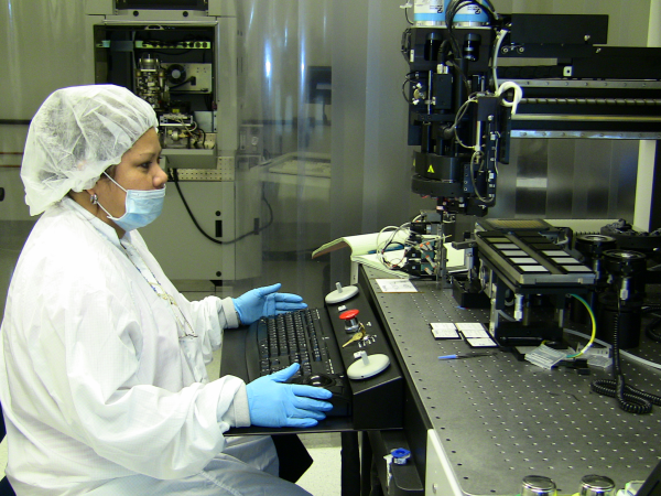
Automation also is often the ONLY way complex packaging can be performed. For example, Multi-Chip Modules (MCMs) in excess of 20 components per part and 100 wires per module are typically automated. Operators can usually handle die sizes larger that 1mm, while automated equipment can handle die sizes below 250 microns. Automated wire bonders can usually attach more than 5 wires per second whereas manual bonders typically process one interconnect every 5 seconds. Even so, for most complex microelectronics, manual adhesive dispense is not an option.
The Lab Considerations
In the Palomar Microelectronic's Contract Assembly lab, the following considerations are taken into account to keep the process rolling along rapidly and accurately:
• Equipment/material certifications performed daily
• Packages or Substrates presented in boats or trays that hold lots of parts
• Piece part presented in ways that reduce work stoppage and yield loss
• Good communication between the process owner and the operator
• Process documentation that is easily accessible
High Accuracy Packaging - Where the Time Goes...
In performing high accuracy packaging, there is often more time spent on engineering: developing processes and defining daily equipment certification requirements and part presentation methods. Looking back to our automation discussion, the time spent on engineering is vital to ensuring as little intervention as possible, by the engineers, once the production begins. The engineers spend much time creating a process that can be supported with little intervention. Our operator and technician can then run production on several machines at the same time. This is high point of efficiency in complex micro-optoelectronic packaging.
Next week
Our next entry will look at a Case Study: an U.S. hybrid microelectronic packaging firm lost its Asian high volume assembly partner, and had to search for a new high volume partner. The search ended in pleasant surprise - a location that was in extraordinarily close proximity to the U.S. firm.
- Don Beck, General Manager, Palomar Microelectronics