Palomar recently exhibited at two very high tech shows in Florida: Electronics Component and Technology Conference (ECTC) and the International Microwave Symposium (IMS). Both shows were very well attended and we had the opportunity to meet people from many different companies and areas of expertise. Inevitably the following question would get asked multiple times a day: “Does your die bonder perform flip chip?” The answer would always be a quick “yes”, but follow-up questions need to be asked in order to help understand exactly what process the system is needed for.
For years, “flip chip” pretty much meant one thing—C4, solder bumps. Wikipedia explains it this way: “Flip chip, also known as controlled collapse chip connection or its acronym, C4, is a method for interconnecting semiconductor devices, such as IC chips and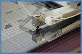 microelectromechanical systems (MEMS), to external circuitry with solder bumps that have been deposited onto the chip pads. The solder bumps are deposited on the chip pads on the top side of the wafer during the final wafer processing step. In order to mount the chip to external circuitry (e.g., a circuit board or another chip or wafer), it is flipped over so that its top side faces down, and aligned so that its pads align with matching pads on the external circuit, and then the solder is reflowed to complete the interconnect.”
At a top level, flip chip involves three critical steps:
- Die is picked up and placed on a "flipping device"
- Die is "flipped" and moved to hover over the substrate (or board or carrier) where bumps reside - precisely positioned in their previously defined positions
- The tool then places the die on the bump with a programmed amount of force
As with most processes in this industry, the flip chip category has grown and expanded over the years to include new technologies and methods. Some examples include thermo-compression, thermo-sonic, and conductive and non-conductive epoxies. Even Wikipedia has expanded the definition a bit: “Since the flip chip's introduction a number of alternatives to the solder bumps have been introduced, including gold balls or molded studs, electrically conductive polymer and the ‘plated bump’ process that removes an insulating plating by chemical means. Flip chips have recently gained popularity among manufacturers of cell phones, pagers and other small electronics where the size savings are valuable.”

Now back to the question, “Can Palomar’s bonders perform flip chip?” The quick answer is yes, we can do many of the processes previously mentioned, including the C4 process. We are known as the “Swiss Army knife of die bonders”—able to perform many different processes and applications. The question now is, are we the best fit for your flip chip application? Stop by our booth at SEMICON West in July to discuss with your application with us, booth #5952.
To learn more about flip chip assembly, check out this article.
|
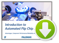
Download the "Introduction to Automated Flip Chip Assembly" eBook |
Download the "Introduction to Automated and Semi-Automated Die Sorting" eBook |
|
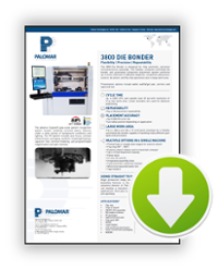
Download the 3800 Die |

----
Dale Perry
Regional Account Manager, Eastern Americas
Palomar Technologies, Inc.