Scaling Semiconductor Manufacture for Space and Beyond
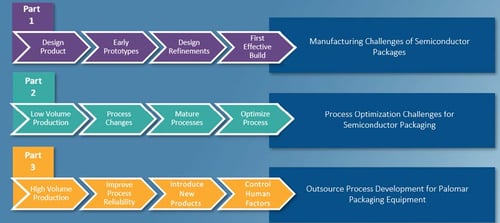
Download the Article!The journey from concept design to full-scale semiconductor manufacturing is often hindered by a number of different obstacles from diverse teams scattered across the world who simply do not understand how the manufacturing process of die bonding, wire bonding or vacuum reflow impacts the package design.
Often, start-up companies or divisions of larger companies may not have a complete team available and might not be aware of how to take their package from design to full-scale production.
Download to read more...