Micron Level Placement Accuracy for Wafer Scale Packaging of P-Side Down Lasers in Optoelectronic Products
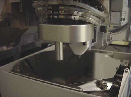
Download the Paper!Applications requiring ultra high placement accuracies of ±1μm to ±3μm are resurfacing in several optoelectronic applications such as Arrayed Laser Print Head and Multi-Channel Optical Communication products. Some of the higher performance optical communication products rely on P-side down laser attachment. This paper reviews measurement, materials, and processes required to successfully achieve ±3μm accuracies for P-Side down laser attachment at wafer level for Chip to Wafer (C2W) or Die to Wafer (D2W) eutectic solder attachment.
Download to read more...