Gold Planar Bumps for Flip Chip Bonding with Challenging Specifications
Semiconductor packaging industry seeks smaller, faster packages. Au Planar bumps are a challenge, explored in this case study.
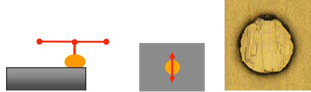
The semiconductor packaging industry continues a relentless pursuit to make smaller packages with higher throughput. The industry demand for smaller components requires manufacturers to adapt by developing new processes. Achieving consistent, quality Au Planar bumps has been a challenge that the industry has been trying to meet for years. In this case study, we explore these shrinking specifications of wire bonding requirements in regards to ball bump mashed ball diameter and top heights for flip chip applications and how to achieve them.