The journey from concept to full-scale semiconductor packaging is often hindered by a number of different obstacles along the way including everything from diverse teams scattered across the world to simply not understanding how the manufacturing process of die bonding, wire bonding or vacuum reflow impacts the package design and vice versa. Often, start-up companies or divisions of larger companies may not have a complete team available and might not be aware of how to take their package from design to full-scale production.
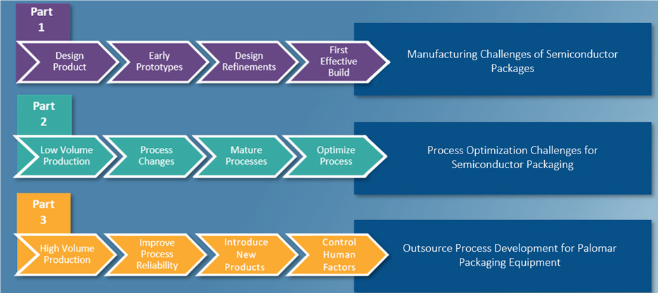 Figure 1: Three Stages of Manufacturing Ramp-Up
The biggest misconception is the belief that going from an initial design to a first article build is an easy one step process. Producing that first build; getting it functional; getting it to be exactly what is desired is not straightforward.
There are several steps to go through; perhaps there is a need to go through multiple builds. There will be learnings about design issues, which may be material or process based; and the designs may need to be changed or refined to be able to get that first effective build.
It’s very important to understand that creating a successful package requires more than one or two build quantities. Several build quantities will be necessary because there is going to be a great deal of learning and discovery about the manufacturability of the package, the materials selection and the process to manufacture. Keeping all this in mind will ensure less wasted time or extra cost. Ordering sufficient build quantities at the outset is advised to prevent waiting through multiple long procurement cycles. To mitigate those risks requires focusing on achieving a minimum viable product.
Once a semiconductor package has been successfully built and tested at low volume, there will likely be some potential areas of improvement within the manufacturing processes. Making processes changes in light of feedback from early product batches will move the manufacturing towards a mature process but can often result in some negative impact in the short term rather than positive impacts. Anytime a process change is made, there will always be new elements of the process to optimize or re-optimize. This typical pattern is represented in Figure 2. As there are many possible process changes and options for improving throughput or yield, ensuring the best path may be difficult, especially for new and evolving products.
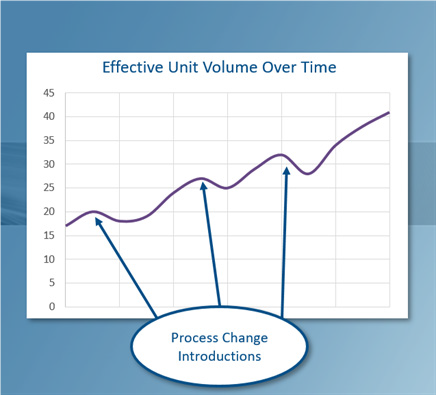 Figure 2: Simplified Effects of Process Change
There will always be a cycle of process development where a mature version of the process will help to identify potential areas for improvement – which in turn will necessitate process changes that require optimizations before effective increase in production volume is seen. After the process matures again, new potential improvements will likely be found.
Last, as a product enters high volume production, continuous improvements are made regardless of how robust or mature the process is. These improvements are driven by process data or from mitigating potential risks that can stem from a variety of factors. Within a stable production, it is often difficult to introduce changes into the process or develop new products or iterations. There is a constant risk of production faults occurring from peripheral influences, such as process personnel. In order to ensure optimal full-scale production of your product, it is imperative to understand the challenges present at this point in the production life cycle.
To learn more about the challenges faced from package design and prototyping, through process development and process optimization, download our 3-part article: The Journey to Full-Scale Semiconductor Packaging Manufacturing and learn how to ensure the device can indeed be manufactured with the desired throughput and quality.
Download these resources for more:
| The Journey to Full-Scale Semiconductor Packaging Manufacturing Paper | 3880-II Die Bonder Brochure | 8100 Wire Bonder Brochure |
 |
 |
 |