In part three of our series on Packaging Technologies meet Quantum Opportunities, we present an overview of how KETS Quantum Security, Bay Photonics and Palomar Technologies are working together to ramp up volume for the miniaturized, integrated photonic platform designed by KETS.
 We live in an era of connectivity and we rely on that connectivity for everything from checking social media and online banking all the way to controlling critical infrastructure and even connecting entire smart cities. Today, millions of devices are connected and communicating as a whole, interconnected system, sending information, gathering data via sensors and sending streams of information.
However, this interconnectivity is proving to present as big of a challenge as the benefits it presents. National governments around the world are warning that with the advent of quantum computing, the convenient cybersecurity tools we use today across the web and beyond have a rapidly approaching expiration date. Over the past few years, Bay Photonics and KETS have demonstrated a range of technologies for quantum-secured communications capable of securing our data in the 21st century. Specifically, Bay and KETS are working together to provide practical photonic driven quantum security solutions to a world in which data is being increasingly targeted by criminals and rogue state security services.
Bay Photonics specializes in providing photonic integrated circuit (PIC) packaging solutions enabling the sophisticated but delicate semiconductor-based integrated circuits to be able to interface practically with the harsh environmental conditions of the real world, providing power, optical interface as well as thermal control and hermiticity. Bay Photonics’ capabilities include die and wire bonding, fiber optical alignment and hermetic sealing. Bay Photonics also provide packaging design services, prototype and pilot build, as well as transfer to volume manufacturing.
KETS Quantum Security is a multi-award winning start-up from the Quantum Engineering Technology Labs (QETLabs) at the University of Bristol. As one of the first companies to spinout of the UK National Quantum Technology Programme, KETS is producing future-proof, scalable, and easily deployed quantum-enhanced solutions. The company is building on almost 20 years’ of world-leading research at the University of Bristol and has developed some of the world’s first integrated quantum secured encryption technologies – from quantum random number generators to full quantum key distribution devices.
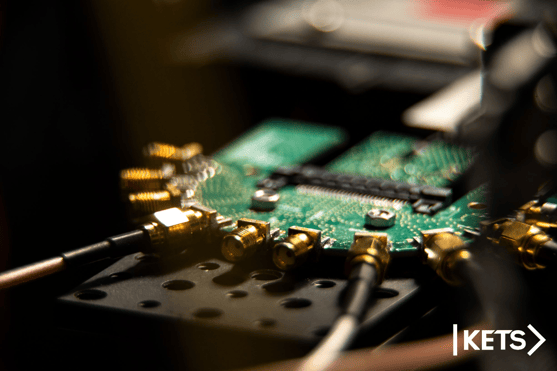 Figure 1. KETS’ integrated photonics chips allow flexible, cost-effective & robust solutions to be deployed at scale even in the most challenging environments
As cities around the world become more and more connected, the capacity demand on networks is expanding enormously. The reality of both increased demand for faster connections, and higher bandwidth to handle the larger volumes of data passing through networks must be met with attractive solutions. For example, by 2025, data centers are expected to consume 4-5% of the world’s electricity[1].
The energy required to power and connect our technology is enormous. However, nobody wants to increase the power consumption or size of their data centers, and customers want scalable and future-proof security solutions that are affordable. The miniaturized, integrated photonic platform (Figure 1) designed by KETS provides the low size, weight, power and cost (SWaP-C) benefits that consumers are demanding. By miniaturizing the device, power consumption is reduced, and by integrating with current semiconductor technology, it can be very cost-effective as well.
Design for manufacturing is Bay Photonics specialty and combined with Palomar Technologies, a leading supplier of automated assembly workstations, KETS’ cutting-edge technology is now being prepared for volume deployment and production.
Palomar Technologies provides automated packaging equipment designed to automate the world’s complex microelectronic and photonic assembly processes. Through delivery of turnkey bonding equipment, the Palomar total solution enables a seamless transition from concept to production in a competitive time-to-market framework. Palomar’s Innovation Centers around the world utilize Palomar’s own equipment and specialize in contract manufacturing and process development to help photonics companies make a seamless transition to high volume production.
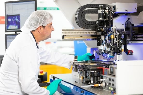
Figure 2. Bay Photonics engineer loading Palomar 3880 fully automatic, high accuracy die attach workstation
Palomar provides a range of flexible packaging solutions for photonics applications. The Palomar 3880-II Die Bonder is the well-known industry standard solution for eutectic, epoxy, UV and flip-chip die bonding. With clever hardware options like in-situ atmospheric plasma cleaning, to insure maximum mechanical strength of all optical components in the optical chain, combined with Palomar’s powerful VisionPilot® radar alignment software, for tricky, low contrast optical lenses, means the 3880-II can really squeeze the best performance out of any packaging materials.
To get maximum performance, linking multiple Palomar bonding solutions together can take product assembly to the next level in terms of first pass yield and ultimate product performance. For example when combining the Palomar 8100 Wire/Ball Bonder to feed the 3880-II with accurate planar Au ball bumps in preparation for successful PiC flip chip thermos compressions applications, this is cutting edge, innovative processing at its finest. Quantum devices are super sensitive to temperature change, so when combo bonding and initially utilizing the 3880-II to enjoy 5μm XY TEC and CoC accurate tack bonding, packages can then be fed into the SST 8300 Automated Vacuum Pressure Soldering System for void free, high-reliability, high-thermal stability results.
Palomar has the advantage of 25 years of optical transceiver automated assembly experience and mastery to take into this quantum market, so companies can hit the ground running to get the correct solution for their innovative applications.
For more information on the assembly of quantum packaging, download these resources:
| 3880-II Die Bonder Brochure | 8100 Wire/Ball Bonder Brochure | 8300 Series Automated Vacuum Pressure Soldering System Brochure |
 |
 |
 |
[1] https://data-economy.com/data-centres-world-will-consume-1-5-earths-power-2025/