Much of the semiconductor packaging industry is engaged with an exciting and growing photonics ecosystem. Anticipating seven percent CAGR over the next five years, this clearly outpaces most other manufacturing sectors. That having been said, the silicon-photonics sub-sector is expected to grow by over five times that amount (c. 40% CAGR) in the same period. More importantly, the underlying fundamentals mean that this is more than sustainable.
The source for this dynamic comes the fact that silicon photonics is a key enabling technology. It is paving the way for a significant step-change in the evolution of a large number of existing and new devices together with the advanced infrastructures necessary to support them. This includes datacenters, edge and cloud, 5G, almost innumerable sensor types, including LiDAR and 3D optics, together with first generation commercialized quantum devices. It is critical to underscore the factorizing present as these technologies interact; they are exponentially key and enabling.
For example, sensors are driving the development of advanced algorithms, which is driving quantum computing, which in turn is driving a new generation of sensor, which is pushing algorithm development towards true AI, in turn pushing computing advances. There are other impacts. While true quantum computing is not expected before 2030, the final certainty of success has made quantum encryption a current imperative. So much so, that photonics-based quantum encryption is already being scaled into high-end smartphones—along with LiDAR.
While exciting, these additional technologies will result in even higher exponential demands on data provision. Doubling every three years, this trajectory has been significantly amplified by the demands of COVID management and growing global competition in ultra-tech. While the pressures on the infrastructures are clear, a far, far greater urgency lies in simultaneously reducing power consumption. Taking 6.5 percent of global energy production and growing, this is clearly unsustainable. Fortunately, the use of different materials provides a solution. Silicon, which is increasingly being integrated for use in photonics, and GaN, which as well as increasingly being used in RF devices, delivers both very significant power reduction and improved performance.
This only leaves us to meet the associated packing challenges—that are also growing. With particular reference to optical transceivers, we particularly note the following:
• Component and device integration.
• Greater speed and capacity.
• Still lower power consumption.
• Homogenous silicon PICs.
If the demands requirements to meet performance gains are technically clear, the reverse side is machine/software capabilities that can efficiently negotiate these—both today and over the medium term. Perhaps the most urgent obstacle is how to squeeze large package functionality into smaller, more thermally efficient, footprints.
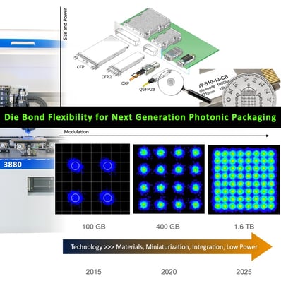
Straightforward to state, but pragmatically, solutions must negotiate through shifting complexities: A typical next gen 100 GB optical transceiver requires 30 or more processes to assemble, using 70 components, and five bonding techniques. In short, we may find ourselves combining eutectic die attach, solder reflow, dual epoxy dispense, epoxy daubing, and flip chip and EV bonding. Besides these techniques, the machine itself must also provide for placement accuracy, repeatability across a large work area, a perfect balance of throughput, together with adaptability and upgradability, modularity and software advances. Finally, and perhaps the biggest challenge of all, the entire process must stretch across all stages of the concept-to-consumer pathway; research, development, new product and innovation, commercialization and volume production.
With Palomar’s history rooted in the Hughes Aircraft Corporation, an initial learning curve built around the demands of aerospace/defense, subsequent innovation born of the heady days of the telecoms boom, and post-boom reorientation, the company has a proven record of effective solution provision. This is little better reflected than in the 3880 die bonder series. The machine and its predecessors have been used for proven mass production across the globe for decades within datacom, telecom and currently 5G markets. The current model has been adapted and tuned to meet a variety of contemporary bonding options, material presentations and automations of process.
Additionally, Palomar’s packaging solutions have been designed to extend from die bonders, to wire bonders, to vacuum reflow systems, each representing not only seamless synergy and various automation options, but a flexibility providing for performance edge, manufacturing and commercial advantage. The following represents a potential system configuration for the assembly of data-center device packaging solutions:
Palomar’s 8100 ball bonder with a large work area, served by precise dual Z-axis Z rotary and Z linear movements, allows the delivery of repeatable planar ball bumps within tight metrics. Packages then feed into the 3880 for the delivery of high-yield PIC Flip Chip thermo-compression. Finally, the SST 8300 vacuum reflow machine works to 5um placement accuracy for TEC and CoC tack bonding. The result is an integrated, high performance, efficient and void-free process. As we have just implied, depending on the device, various levels of automation are possible, from full to partial. Any would-be solution must meticulously designed in advance to meet the requirements of technical and commercial optimization.
Looking ahead to the rest of the decade, Palomar believes the following represent the most acute ecosystem requirements:
• Relentless drive to miniaturization.
• More keep-off areas.
• Increased PIC structure complexity.
• Move away from expensive hermetically sealed packaging.
• Greater optical alignment automation.
• Increased diversity of sourcing/changing supply chains.
It is these same best practice qualities that Palomar seeks to reproduce in our global Innovation Centers, allowing smaller and medium-sized companies and academic institutions to work with us while leveraging big-company advantages. Our center in Paignton, England recently faced the challenge of using low mechanical strength and UV snap cure epoxies. The problem faced was a low yielding optic bond process. By applying in-situ atmospheric plasma cleaning directly before UV Epoxy die bonding, we were able to ensure that bond shear strengths were accurate and repeatable throughout the course of the shifts production. This resulted in marked improvement in batch yields.
More and more, successful outcomes are the result of co-creating solutions with our customers; an activity around which these centers have been designed. Strategically located to support Asian, North American and European markets, each provides for manufacturing and assembly, rapid prototyping, process development and contract services. Our latest center in Paignton is new build facility constantly adding additional capabilities. Sited within south west England’s advanced photonics cluster, it is also a hot spot of local collaboration.
To learn more about die bond flexibility for the assembly of next-generation photonics packaging, register for our webinar, April 28 at 8am PDT or 4pm BST hosted by Kyle Schaefer, Palomar Product Marketing Manager and Martyn Davies, Palomar Business Development, UK. They will take you on a journey of how to successfully assemble photonics packaging, followed by a live tour of the Palomar Demonstration Lab in Paignton, UK.
Download these resources for more information:


