WIRE BONDING

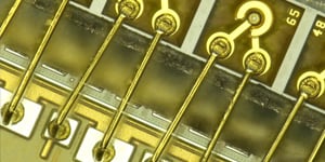
Gold wire bonding is the process by which gold wire is attached to two points in an assembly to form an interconnection or an electrically conductive path. Heat, ultrasonics, and force are all employed to form the attachment points for the gold wire.
The process of creating the attachment point begins with the formation of a gold ball at the tip of the wire bond tool, the capillary. This ball is pressed on the heated assembly surface while applying both an application-specific amount of force and a frequency of 60kHz - 152kHz of ultrasonic motion with the tool.
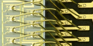
Once the first bond has been made, the wire will be manipulated in a tightly controlled manner to form the appropriate loop shape for the assembly’s geometry. The second bond, often referred to as the stitch, is then formed on the other surface by pressing down with the wire and using a clamp to tear the wire at the bond.
Gold wire bonding offers an interconnection method within packages that is highly electrically conductive, nearly an order of magnitude greater than some solders. In addition, gold wires have a high oxidation tolerance compared to other wire materials and are softer than most, which is essential for sensitive surfaces.
The process can also vary based on the needs of the assembly. With sensitive materials, a gold ball can be placed on the second bonding area to create both a stronger bond and a “softer” bond to prevent damage to the surface of the component. With tight spaces, a single ball can be used as a starting point for two bonds, forming a “V” shaped bond. When a wire bond needs to be more robust, a ball can be placed on top of a stitch to form a security bond, increasing the stability and strength of the wire. The many different applications and variations to wire bonding are nearly limitless and can be achieved through use of the automated software on Palomar’s wire bond systems.
Resources for Gold Wire Bonding:
CONTACT US TO DISCUSS YOUR PROCESS CHALLENGES