RF GaN’s Millennial Progression
Since the early 2000s, the RF market has witnessed significant amounts of investment (individual, industrial corporate, venture capital) in GaN technologies. Some of it is in “big name” companies, but a surprisingly large portion has gone into startups and other newer entrants, but most especially university spin-offs (for reasons we shall identify in a moment). The key players in RF GaN have been developing the technology for well over 15 years, and built up a significant bank of knowledge, expertise, and competence—but above all, an almost evangelical sense of belief in the long term value of the technology. On account of the highly specialized nature of the research, however, much of it has been done in collaboration with the world’s best research universities. This in turn meant that key findings were placed in the public domain through academic papers. A number of post-graduate students working in this field became so fired up by the technology that they decided to commercialize it for themselves. And so, we have now accounted for the large number of university start-ups in RF GaN relative to other scientific disciplines. Collectively then, hard work, determination, and a sharp strategy of commercial exploitation are beginning to bear fruit for companies large and small.
That having been said, just as RF GaN assumes an increasing air of mainstream and concept turns into real products, the thinkers behind the scenes continue to think. The new areas of research range from experimentation with alternative or additional materials to use with GaN—such as diamond—to full component integration, RF’s equivalent to photonic-in-package technologies (the photonic integrated chip).
Innovations in Material and Scale
At the other end of the technological horizon, development work continues among some manufacturers as they examine fabricating RF GaN products using existing, legacy technologies—but experimenting with new, cheaper materials and building scale for volume and cost-reduction in the wafer fab. The goal is to create a commercially viable range of RF GaN technologies that are cost effective versus their LDMOS and GaAs alternatives. While these are not seen as long term products, they are an invaluable bridge to the next generation. Furthermore, with the pace of invention and innovation seemingly accelerating, they may, in fact, prove a better choice.
MACOM MAGb, GaN-based Power Transistor
MACOM’s MagB power amplifier is a good example of GaN on Si showcasing cost parity with traditional LDMOS technology while delivering improved performance.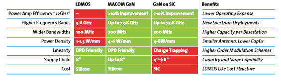
Figure 1: GaN on Si performance and cost vs. LDMOS, source: MACOM MAGb product brochure
Predictable Fallout of Technological Innovation
Building on the general commercial principle that technology follows a definable pattern of investment, application, new applications/end uses, industry adoption and wide commercialization, the graphic below applies this pattern of RF technology. Advanced technology usually begins with high sensitivity to performance and then moves into cost sensitive territory once the technology is stabilized and widely adopted. The upper right-hand circle indicates RF GaN edging into sectors previously dominated LDMOS and GaAs applications.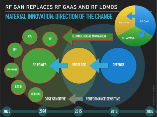
Figure 2: Performance to Cost Sensitive movements, source: Dr. A. O’Sullivan, 2016
Forces of Innovation
Over the past 18 months it has been increasingly evident that the roll-out of 5G wireless has been the dominant force drawing the more recent tranches of investment into RF GaN transistor development. With specific—and now very tight dates—in the public domain for national implementation of 5G (covering more than half the globe) by the end of 2020, together with significant public money boosting the development of SMART cities, health technologies, as well as zero emission vehicles, it is now expected that half a trillion dollars will be invested in these technologies by 2023. A significant portion of this money will find its way into the further development of RF GaN technologies, new materials, and processes. Similarly, the primary demand accelerating GaN on SiC and GaN on Si power devices for other applications such as solid state cooking, vehicle plasma ignition, agricultural drying processes, lighting, and so on, will draw additional investments.
Global Drivers of RF GaN Technology:
• A number of European Union countries and the United Kingdom have mandated that all vehicles must be emission-free by 2040 or earlier (air quality).
• It is anticipated that China and a number of other Asian countries will follow suit either on a city or regional basis, or nationally.
• In both cases, demand for RF GaN technologies is further supplemented by the required infrastructure provisions as well as concomitant push for the development of autonomous vehicles and drones.
• In 2017 alone, well over US $1 trillion in government expenditure was announced for 5G ecosystem build out for “Smart Nations”, “Smart Cities”, “Smart Health”, etc.
• Finite amount of spectrum availability (will see increasingly Massive MIMO combined with higher frequency power amplifiers to drive more into spectrums available and into the expected opening of sub-6 GHz).
• Artificial Intelligence, Augmented Reality, and what is anticipated as a vast number of Sensing technologies—some of which will require low latency for mission-critical end-use applications—will all drive further demand for RF GaN technologies..
• Governments are stepping up their renewable energy efficiency mandates as their respective populations’ power demands increase; this relates not only to the production of eco-power but also its storage (battery farms).
• Industry’s need to reduce energy cost to improve competitiveness, relevance and good-will with consumers.
• National prestige, defense, technology and security issues are leading to significant government investment in local, autonomous research budgets to develop the ultra-tech dimension of RF GaN (and other) technologies.
Considering the global 5G ecosystem, and not least its anticipated rapid evolution, the critical nature of RF GaN technologies is self-evident. This is true across the entire range represented by 5G, but most especially in regards low latency, mission-critical requirements along with the urgent drive for energy efficiency. In each of these respects, GaN’s inherent properties deliver: higher frequency, higher voltage, input power robustness, wire band performance, improved efficiency, and reduced form factor size (up to ten-fold).
Figure 3: the evolution of 5G networks requires the kind of performance only possible with RF GaN technologies; source: Macom, Qorvo and others.
Assembly and Packaging RF GaN devices
RF GaN found its first applications in military and defense fields (as noted in Figure 2) due to its significantly higher performance across a range of factors. Given the mission critical nature of the applications, cost issues were decidedly secondary. Driven by a plethora of advantages, research and innovation has allowed GaN to become commercially mainstream to the point where cost-sensitivity is becoming more an issue with each year that passes. LDMOS and GaN die bonding and wire bond suppliers for RF devices must be cognizant of this critical lateral shift. Furthermore, the introduction of new materials for ‘attach’ as well as the substrates themselves, may have considerable further impact on commercial viability.
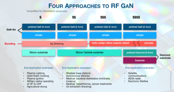 Figure 4: simplified representation of four approaches to RF GaN; source: R D Hueners.
Device Cost and Performance
High power RF packaging and assembly anchor processes rest with the automated die bonders, capable of high-speed GaN Ag Sintering dispense and high throughput of GaN AuSn eutectic assembly -- critical to realizing full commercialization. Equally, device performance remains fundamental and maintaining profitable yields. To help fulfill these criteria, bonders need to utilize enhanced software to control the Ag sinter bond line thickness (to ensure void levels are very tightly controlled), and a high level of force control to successfully handle the smaller package elements. As GaN packages have greater density compared to their LDMOS and GaAs counterparts, outstanding process control is the only way to deliver high yields.
Passing Zone: LDMOS to GaN
Most analysts agree that GaN and LDMOS will co-exist for the foreseeable future, however, GaN will undoubtedly edge out LDMOS over time. The good news for manufactures is that GaN Ag Sinter, GaN AuSn, and LDMOS AuSi eutectic processes for RF transistors can be packaged using the same machine, though with critically divergent tooling options (as reflow temperatures are different from AuSn to AuSi). For device manufacturers needing a single bonder that can package both GaN and LDMOS across the spectrum of methods, and to the highest required specification, Palomar provides a total RF GaN-LDMOS Sinter & Eutectic Toolkit.
Looking Ahead to 2050
The pressures to provide for smaller, faster, more compact, lower cost, lower power, higher performance, more reliable products, comprise the relentless background of commercial and technological pressures that are increasingly definitive in setting the parameters for these new advanced packaging methods. Ultimately they can lead to only one logical conclusion; the development of monolithic integrated packaging with the final goal of eliminating the line between chip and package. Exactly what this product will finally look like, and the processes necessary to achieve it, are clouded by unknowns. More immediately, however, there will be hybrid intermediate stages which will represent challenges for manufacturers and their vendors alike; but for companies like Palomar, this is the essence of what it means to be engaged in our technological eco-system and keeping practical focus in helping our customers remain leaders in their markets.
Learn about Palomar’s advanced packaging systems for RF GaN:
| Download the 3880 Die Bonder Data Sheet | Download the new 6532HP Die Bonder Data Sheet |
 |
 |
----
Dr. Anthony O’Sullivan of Palomar GmbH
Richard Hueners
Vice President, Global Sales
Managing Director, Palomar Technologies (SE Asia) Pte Ltd
This blog examines current trends in the RF GaN packaging eco-systems. Our aim has been to give our readers a glimpse into the technology’s future, as well as hints regarding Palomar’s own roadmap. The views represented are entirely those of the authors, Richard Hueners and Dr. Anthony O’Sullivan of Palomar Asia and GmbH respectively. Richard Hueners and Dr O’Sullivan will gladly field questions and comments.