With the increased demand for improved functionality and miniaturization in portable hand-held devices—such as cell phones, PDA, digital cameras and laptop computers—original equipment manufacturers (OEMs) and integrated device manufactures (IDMs) have joined forces to ensure enhanced chip performance without sacrificing valuable board real estate. Rather than use conventional single chip or multiple-chip type packaging, chip designers have turned to the assembly houses for multiple die stacking solutions. Stacking of die, such multiple memory chips, not only provides a reduction in overall package footprint, but a substantial improvement in electrical performance through quicker transmissions requiring less energy to drive the signals. This extends Moore’s Law and enables a new generation of tiny but powerful devices.
With cell phone subscribers increasing to over 5 billion, there is at least one stack-die assembly in every phone sold. Die stacking—or 3D-IC packaging—has become common place among leading semiconductor manufacturers, even as the assembly houses continue to be faced with challenges as the die stacking becomes more and more complex. In order to increase functionality, the number of die stacked can range from 2-18 integrated circuit devices (ICDs) as reported in current device applications.
Die stacking requires all known-good-die (KGD) to be thinned and bonded on top of each over in either an overhang pattern as shown in first figure below or a pyramid stacking as shown in the second figure. As a cost saver, most die stacking is typically wire bonded to form the interconnection within a standard package.
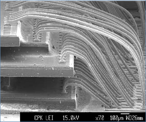 Die Stacking with Overhang
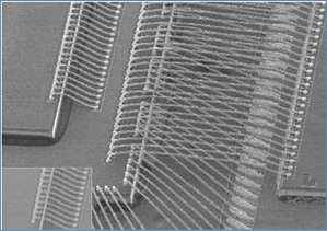 3D IC Pyramid Assembly
There are risks associated with stacking two or more KGD together, since one KGD can function independently well, but within a stack assembly it may not as effectively. Rework may be required to remove the bad die or the entire stack-die assembly may be bad together. In addition, heat dissipation with large stacks can be a concern and risk factor as well. However, the advantages of the high level of functional integration achieved by mixing complex semiconductor chips—such as a MEMS (electro-mechanical systems) or silicon ASIC chips—with stacks of memory chips far outweigh the risk.
To reduce some of the risk in die stacking, packaging expertise is required to assemble multiple die within a single footprint. Each stack configuration requires precision die bonding for both the pyramid stacking and overhang die stacking. If die are not aligned properly during the bonding step, there may not be enough room to wire bond to the adjoining die pads. This becomes comes more apparent as the tolerances decrease with each die stacked. In some cases, die alignment better than +/-4μms must be achieved during the die bonding.
Once the die are bonded together, many factors must be weighed before commencing to wire bond the package. Stack-die bonding requires the most advanced bonding techniques within a single platform such as low loops, chain bonding (multiple-tier) and/or stand-off-stitch (SOS). For each bonding technique, optimization of the applied bonding force and trajectory of the loop formation must be achieved and maintained. If too much force is applied, die deflection can occur, resulting in potentially cracked die or damage to die pad metallization. In addition, the design of capillary is also an important factor to consider when bonding a die stack.
How far will die stacking go? It is tough to say. Some never thought die stacking would go beyond four devices. Through technology advancements of TSVs (Thru-hole Silicon Vias) combined with wafer-level packaging (WLP), the assembly house will play a critical role in the coming years on just how far a die stack assembly can go to achieve the optimum performance and functionality.
Download these resources for more information:
|
Improved Wire Bond Reliability eBook
|
Chain Wire Bonding of a RF SOE Package Using a Gold Ball Bonder Technical Paper |
8000i Wire Bonder Data Sheet |
Assembly Services Data Sheet |
6500 Die Bonder Data Sheet |
3800 Die Bonder Data Sheet |


----
Julie Adams
Director of WW Sales, Assembly Services
Palomar Technologies