Continuing on with our overview of microelectronic interconnection methods, we will discuss three additional methods: Solder Bump Bonding, Ball Bumping Materials, and Wire Bonding.
Solder Bump Bonding
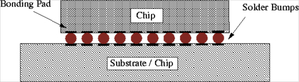
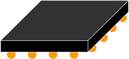
Solder Bumps are the small spheres of solder (solder balls) that are bonded to contact areas or pads of semiconductor devices. Subsequently, they are used for face-down bonding. The length of the electrical connections between the chip and substrate can be minimized by:
- placing solder bumps on the die
- flipping the die over
- aligning the solder bumps with contact pads on the substrate
- re-flowing the solder ball in a furnace to establish the bonding between the die and the substrate
Ball Bumping Materials
A few key points on ball bumping materials. The primary bump material still used is solder. Solder Bumps are fabricated by evaporation, plating and solder screening. Depending on your application, you may choose an alternative bump material. These include gold stud bump, conductive epoxy, copper balls or columns. For more on the Ball Bumping process and how it works, check out Wire Bonding - Gold Ball Bumping. If your interest in is an actual Ball Bumping machine, you can read about Palomar's 8000 Ball (Stud) Bumper which also can be configured as a wire bonder.
Wire Bonding
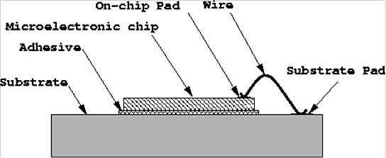
Most people know wire bonding, so I will just scratch the surface. The basics: Wire Bonding is a method used to connect a fine wire between an on-chip pad and a substrate pad. This subsrate may simply be the ceramic base of a package or another chip. Common wire bonding materials include gold and aluminum (Al is often used in wedge bonding). Highly specialized applications that are subject to government regulatory approval, such as implantable medical devices, may require using platinum wire for the wire bonding. For more about wire bonding, visit Palomar's more in-depth wire bonding webpages.
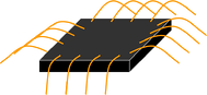
Here is a very simple rendering of how a wire bonded package looks:
Putting Interconnection Methods Together
Depending on your application and the goal of your end product, you will have different requirements. For example, you may need a smaller package. Or, you may need more power and reliability and in exchange will work with a larger package, for the package size doesn't matter. Today, many applications require a very small package with all of the power and reliability benefits of a larger package. Regardless of your need, Palomar engineers continually say "bring us your challenge". If your application requires high power and high reliability, Palomar is the best in the business.
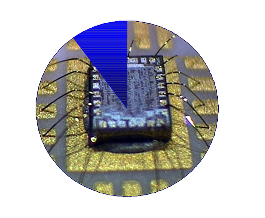
IC with Wire Bonds Same IC with Bump Connections
Taking these two bonding methods and putting them together is a very common application. The below picture is ~10% BALL CONNECTIONS and ~90% Wire Bond connections.