Often when companies are discussing potential projects, they are at a crossroads on the most economical way to proceed with a small quantity of prototype parts. They are looking for a way to prove out the concept or win their potential customers’ business without breaking the bank.
For a flip chip device, the question could be between bumping a die with gold ball bumps and using this method of interconnect vs. spending the thousands of dollars to get a wafer plated/solder bumped. The former can be a viable path forward, and indeed can be quite a bit less expensive. However, it’s not without its challenges.
Bumping Challenges
We need to consider some of these challenges for bumping the die. First, fixturing the die, keeping in mind that we are applying heat and ultrasonics to form the ball bumps; and then the “shearing” of the bump itself after the bond is formed. This requires the die to be adequately held using vacuum or mechanical clamping, preferably both. The easiest way to do this with small die is to do it in wafer format, or at least in partial wafer format, and singulate the die after the bumping has been completed. Trying to fixture individual die can be a challenge and would probably require custom tooling and additional handling, ultimately increasing the price.
The bump diameter and height also needs to be considered. Remember, taking a 25-50 micron wire and forming a ball requires a ratio that needs to be kept in mind. A typical 25 micron wire will result in approximately a ball diameter twice the size and about 2/3 of the diameter heights. This is just a general guideline as with the right ball bumper, there are “tricks” to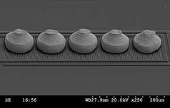 achieving variances to this, including “stacked bumps”. The Model 8000i Wire Bonder has a lot of flexibility and the dual axis bond head gives it some capabilities for ball bumping that no other systems have.
Connecting to the Substrate
Bumping the die is only the first step of the challenge. The end method of connecting the die to the substrate needs to be in mind from the beginning. There are quite a few ways that these bumped die can be connected to the package using Direct Chip Attach (DCA). Probably the most common are thermocompression or thermosonic. However, these methods can require special equipment and, due to the forces required, could present challenges to the components themselves. There are alternative methods that can utilize more flexible equipment sets such as the 3800 Die Bonder.
|
These methods could include anything from conductive epoxy placed accurately and consistently on the pads using the dispensers or daub pot, or a system such as the GPD Max System with a Micro-Dot Pump. There is also the option of non-conductive epoxy that then shrinks during cure, pulling the gold/gold interface into solid connection. Additionally, there is the possibility of utilizing an anisotropic paste or film that would only conduct in the Z-axis. |
 |
All of the above have their challenges and benefits. Characteristics such as pad size, pitch, die size, and number of bumps will also play into the decision as to the best process to achieve success.
Download the data sheets to learn more:
|
3800 Die Bonder |
8000i Wire Bonder |


----
Dale Perry
Regional Sales Manager, Eastern Americas
Palomar Technologies, Inc.