Eutectic bonding of Au-backed MMIC (Monolithic Microwave Integrated Circuits) power amplifiers presents a unique challenge due to the thin, brittle nature of the device and the need for a virtually void free attachment of the backside of the device to the heat sink. Both scrub assisted processes and vacuum solder methods have been successfully employed throughout the industry. The question is: how good is good enough? In the microwave world, the concerns are more than just total voiding under the die which diminishes the ability to draw heat from the component. A small void in the wrong location could be just as critical; therefore, total voiding and the location of the voids should be addressed by the process engineer to assure a reliable die attach.
This blog will briefly review the eutectic die attach process, existing Mil-Std-883 die voiding specifications, along with additional concerns and reliability issues related to high-frequency/high-powered MMIC die attach.
The Eutectic Bonding Process
Scrub assisted automatic die attach is a common process that relies on “scrubbing” of the die into the pad in order break up the oxides and get good mixing to form the eutectic alloy. This type of process eliminates the need for flux. By definition the equilibrium eutectic point is the lowest melting alloy in the binary phase diagram. AuSn (m.p. 280 C) and AuSi (m.p. 363 C) are commonly used alloys. Clean surfaces, good metallization and a flat heat spreader are all critical process engineering concerns. Control of the heat delivered to the stage, amplitude of the scrub cycle, time of scrub and force must all be set correctly and optimized in order to form a good void-free attachment. Selection of a properly sized edge contacting tool for a thinned MMIC die is also another important part of the process.
Flux-free vacuum soldering is also used to form a eutectic bond. Graphite tooling is employed to precisely hold the MMIC die in a place while the unit is exposed to various time/temperature/gas/vacuum profiles.
Die Voiding Specifications
The decision to use eutectic bonding vs. epoxy bonding is generally driven by the power levels of the die, maximum junction temperatures and expected lifetime of the product. Two Mil-Std-883 specifications are often referenced for voiding criteria in high-reliability military and industrial applications. Mil-Std-883 J TM 2012.9 specifies voiding criteria underneath the die. This test method is under review in JEDEC to incorporate the newer, real-time X-ray equipment that is now available in the marketplace. The die attach voiding criteria states that either of the following conditions would be cause for reject:
-
Contact area voids in excess of one-half of the total contact area
- A single void which traverses either the length or width of the semiconductor element and exceeds 10 percent of the total intended contact area. There is a figure in the test method that illustrates the criteria. These voiding criteria may be fine for a lot of products, but is inadequate for high frequency, high power MMICs
Ultrasonic evaluation of die attach per TM 2030.2 is another non-destructive analysis tool that is predicated on imaging a reflected sound wave that passes through the device. Parts are normally submerged in deionized water and the sound wave is captured and processed to produce an image that highlights the unbonded regions under the die. The total voiding criteria is the same as in the X-ray test method, which requires 50% bonded as a minimum. In addition, no single void can be in excess of 15% and no single corner void in excess of 10%. There are some additional voiding requirements based on maximum voiding in any one of four quadrants, but as with X-ray this criteria is not sufficient and needs to be tailored to the specific device type.
|
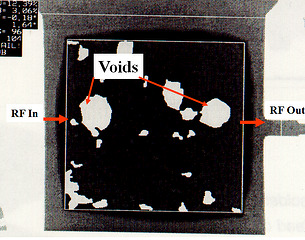
Voids under a high-frequency/high-power MMIC |
 |
Reliability Concerns
The voiding criteria in the two test methods discussed above needs to be expanded and tailored to address MMIC devices. The real concern is location of voids relative to the device features. A relatively large void located directly under the channel region in an FET structure on the die where the heat is generated is much more problematic than a void under a non-active area. On most MMICs there are a lot of non-active regions on the die surface relative to silicon ICs. Under an active area the heat generated will bunch up and the device will fail sooner than expected in the field. Another area of concern is voids underneath the bond pads. A void under a 2 or 4 mil thick GaAs die is a problem for two reasons:
-
The die could crack when subjected to the ultrasonic vibrations of wire bonding
- A void under the RF pathway through the chip could set up a standing wave and be a source of electrical interference at high frequency
Voids underground vias are also cause for concern. It makes sense to overlay the device features onto the X-ray image and highlight the critical areas where no voiding is allowed. The image above displays an X-ray which shows total voiding at 13%; however in this case, the voids happen to be situated in the RF pathway through the MMIC, and therefore presents a potential problem.
|
Solder burst on GaN power amplifier due to excess time/heat during die attach |
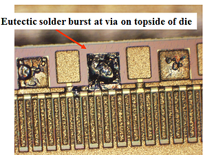 |
Another concern that must be addressed with a visual inspection is eutectic attach material that wicks up into the via and alloys into the gate region. If the process time/temperature profile is too long, this type of defect can easily occur as shown in the image above.
Summary
Reliable eutectic die attach of high-powered/high-frequency MMICs essentially requires a void-free attachment, or as close to a 100% attachment as possible. Certainly 90-95% attachment is achievable with both scrub assist and vacuum soldering, but even then the wrong sized void in the wrong place could become a reliability issue and lead to premature failure in the field.
To learn more about microcircuits and RF microwave material and process development including die attach, wire bond, package seal and associated hermeticity testing, visit TJ Green Associates LLC at www.tjgreenllc.com.
----
Thomas J. Green
TJ Green Associates LLC
For more on eutectic or epoxy die attach, download the eBooks here:
 |
 |